%22%2F%3E%0A%20%20%3Ccircle%20cx%3D%22220%22%20cy%3D%22150%22%20r%3D%22180%22%20fill%3D%22%2322d3ee%22%20fill-opacity%3D%220.12%22%2F%3E%0A%20%20%3Ccircle%20cx%3D%221010%22%20cy%3D%22130%22%20r%3D%22220%22%20fill%3D%22%2338bdf8%22%20fill-opacity%3D%220.08%22%2F%3E%0A%20%20%3Ccircle%20cx%3D%22920%22%20cy%3D%22520%22%20r%3D%22170%22%20fill%3D%22%2322d3ee%22%20fill-opacity%3D%220.06%22%2F%3E%0A%20%20%3Cpath%20d%3D%22M140%20430h920%22%20stroke%3D%22url(%23line)%22%20stroke-width%3D%2212%22%20stroke-linecap%3D%22round%22%2F%3E%0A%20%20%3Cpath%20d%3D%22M220%20360c120-150%20260-220%20380-220s260%2070%20380%20220%22%20fill%3D%22none%22%20stroke%3D%22%2367e8f9%22%20stroke-opacity%3D%220.5%22%20stroke-width%3D%2216%22%20stroke-linecap%3D%22round%22%20stroke-linejoin%3D%22round%22%2F%3E%0A%20%20%3Cpath%20d%3D%22M300%20398h600%22%20stroke%3D%22%2394a3b8%22%20stroke-opacity%3D%220.24%22%20stroke-width%3D%228%22%20stroke-linecap%3D%22round%22%2F%3E%0A%20%20%3Ctext%20x%3D%22220%22%20y%3D%22510%22%20fill%3D%22%23e2e8f0%22%20fill-opacity%3D%220.7%22%20font-family%3D%22Arial%2C%20Helvetica%2C%20sans-serif%22%20font-size%3D%2238%22%20letter-spacing%3D%228%22%3EINSIGHTS%3C%2Ftext%3E%0A%3C%2Fsvg%3E)
Samsung’s AI story has mostly been told through one lens: memory (HBM/DRAM), plus the policy overhang (tariffs) and competitive intensity (e.g., CXMT-style memory moves). The new development is different in kind.
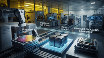
Reuters reports that Samsung Electronics signed a memorandum of understanding (MOU) with Broadcom covering up to $200 billion across memory chips, contract chipmaking, and advanced packaging, extending through 2030. Critically, Reuters says Broadcom’s next-generation communications chips will be made with Samsung’s sub-2-nanometre process technology, and the partners will also collaborate on next-generation HBM products. That package effectively puts Samsung in the role of a foundry + advanced packaging manufacturing engine for a major custom-ASIC customer.
Verified event: scope + mechanics
This MOU bundles memory, sub-2nm logic fabrication, and advanced packaging—so Samsung sells manufacturing outcomes, not just parts
What the Reuters primary source actually says
Time horizon
Through 2030
Agreement described as covering cooperation “until 2030.”
Total value referenced
Up to $200B
Reuters frames it as a pact “envisaged to exceed $200 billion until 2030.”
Where Samsung is involved
Memory + contract chipmaking + advanced packaging
Reuters describes cooperation across these three areas.
Logic node
Broadcom’s next-gen communications chips at Samsung sub-2nm
Reuters explicitly links Broadcom logic to Samsung sub-2nm manufacturing.
Memory product tie-in
Collaboration on next-gen HBM
Reuters says the two will collaborate on next-generation HBM products.
Why this matters: foundry economics (utilization, yield, and node premium) and advanced packaging economics (integration throughput and complexity) differ from memory-only pricing cycles. A bundled, multi-year manufacturing relationship can smooth demand volatility and shift Samsung’s revenue mix toward higher value-add processes—if execution matches the scope in the MOU.
Supply-chain mapping
Full stack transmission: from Broadcom ASIC design choices to Samsung sub-2nm + HBM + packaging throughput
- Upstream/design layer: Broadcom’s custom ASIC/communications designs determine die specs and timing; Samsung’s process platform is then selected as the manufacturing path.
- Node and yield layer: sub-2nm manufacturing at Samsung converts design intent into real silicon; successful qualification is a gating constraint on ramp speed.
- Memory layer: next-generation HBM collaboration links compute die roadmaps to stacked-memory bandwidth needs; this couples Samsung’s HBM demand to Broadcom’s accelerator/communications system roadmaps.
- Integration layer (advanced packaging): the “system” value is realized when Samsung’s advanced packaging can integrate logic + HBM at the required yields and densities.
The economic implication is that Samsung’s customer is not just buying a commodity component; Broadcom is effectively buying a path to operational AI/communications hardware. That path pulls together node execution (sub-2nm), memory supply (HBM), and packaging integration—so Samsung’s performance must be coherent across the stack.
Margin mix thesis
Samsung’s foundry/packaging “quota-share” effect could matter precisely when advanced-node pricing power is rising and alternatives face ramp risk
The brief’s framing argues for a margin-mix swing: Samsung could become more than a memory supplier if foundry/packaging services scale under high-demand AI roadmaps. The event provides the missing link: Reuters explicitly states sub-2nm process technology manufacturing for Broadcom’s next-generation communications chips plus advanced packaging.
Recent fundamentals suggest Samsung has already been able to grow operating profitability, giving it capacity to fund process and packaging execution
Illustrative of Samsung’s profitability level in the last two years of audited financials from the data tool (not a direct measure of margins in the Broadcom deal).
Unit: KRW
FY2024 operating income (KRW)
32,725,961,000,000
FY2025 operating income (KRW)
43,601,051,000,000
FY2024 revenue
$300.9B (KRW 300.9T)
Income statement (FY ended 2024-12-31, KRW).
FY2025 revenue
$333.6B (KRW 333.6T)
Income statement (FY ended 2025-12-31, KRW).
FY2024 operating income
KRW 32.7T
Income statement (FY ended 2024-12-31, KRW).
FY2025 operating income
KRW 43.6T
Income statement (FY ended 2025-12-31, KRW).
Broadcom business model implication
Broadcom’s custom-silicon customer concentration can create a manufacturing “stickiness” advantage—raising execution pressure on both companies
The MOU changes how the relationship is likely managed. If Broadcom is effectively contracting for manufacturing outcomes across multiple semiconductor layers, then delays in qualification, yield, or packaging integration cascade quickly into Broadcom’s own system roadmap.
What to watch next (angles that can be answered with evidence)
Short-term (weeks–quarters) and long-term (1–3 years): the specific signals that validate the foundry + ASIC rerating
- Qualification milestones: look for Samsung and Broadcom commentary on successful tape-out, NPI, and packaging integration timing for the sub-2nm communications chips (validation of ramp readiness).
- Mix evidence: monitor Samsung’s segment/product disclosures for a relative improvement in logic/foundry-linked revenue contribution vs. memory-only narratives (if disclosed; otherwise infer from capex and delivery commentary).
- HBM coupling: expect Broadcom’s system roadmap choices to show up in next-gen HBM collaboration cadence; delays here would imply the coupling isn’t flowing smoothly.
- Packaging intensity: watch for any indicators that packaging complexity is rising (e.g., “advanced packaging” scale-up) because that is where incremental service content can show up even when raw die demand is stable.
Longer term, the rerating hinges on sustained utilization and yield performance at the node/packaging level specified by the MOU. A bundled AI-chip manufacturing relationship can be margin-positive if it reduces customer churn risk and increases advanced-process share; it can also be margin-negative if yield is insufficient and rework costs rise.
Cross-check: where the numeric evidence comes from
Numbers used here come from audited financials; the $200B deal number comes from the Reuters report
| Topic | Metric | Value shown | Source type |
|---|---|---|---|
| Deal scope | Total value and coverage areas | Up to >$200B; memory + contract chipmaking + advanced packaging; through 2030 | Reuters primary source opened in-session |
| Samsung profitability backdrop | Operating income and revenue | FY2024: KRW 32.7T operating income; FY2025: KRW 43.6T operating income | Financial data tool (income statement) |
| Samsung profitability and balance sheet context | Market-level fundamentals | TTM margins and profitability ratios (e.g., operating profit margin) | Financial data tool (company overview / key metrics) |
| Broadcom health snapshot | Market fundamentals context | TTM margins and revenue (context only; not deal-specific) | Financial data tool (company overview / key metrics) |
Listed stocks most plausibly tied to the Samsung–Broadcom manufacturing shift
- Samsung’s MOU explicitly ties Broadcom communications chips to Samsung’s sub-2nm manufacturing path, increasing the chance of mix shift toward foundry/packaging-led revenue through 2030.
- Samsung’s FY2025 operating income rose to KRW 43.6T, giving it capacity to fund node and packaging execution; validation would support the new margin mix narrative.
- If advanced packaging throughput scales, Samsung’s advanced-process content could rise faster than pure HBM-only demand, supporting premium multiples.
- Broadcom’s custom communications ASIC roadmap is manufactured at Samsung sub-2nm under the MOU, so qualification success would lock in supply while delays risk schedule slips.
- Broadcom’s TTM gross margin is elevated (tool snapshot), so if manufacturing outcomes hold, Broadcom can protect system-level gross profit despite higher integration complexity.
- Because this is a multi-year manufacturing relationship, Broadcom’s customer/ship risk shifts toward execution risk management rather than only demand forecasting.
- If Samsung wins share in sub-2nm manufacturing for a large custom-ASIC customer, TSMC loses a potential advanced-node allocation at the margin.
- TSMC’s economics are node-utilization driven; any displacement of demand to Samsung would press utilization and near-term pricing power at the margin.
- Long-term impact depends on ramp yields; if Samsung execution is weaker, demand may re-concentrate toward TSMC.
- Intel’s 18A/advanced node ramp uncertainty matters because Broadcom’s MOU chooses Samsung sub-2nm; that increases the probability that some advanced-node proof gets deferred away from Intel.
- If Intel later proves competitive yields and packaging integration, the “proof gap” could close and reroute future ASIC manufacturing—but that catalyst requires disclosure.
- Near term, the signal is whether Broadcom expands beyond Samsung; until then, Intel’s benefit remains contingent.
- HBM collaboration is explicitly part of the Samsung–Broadcom MOU; that creates a potential allocation constraint on Samsung’s HBM capacity, but it also affects HBM buyers’ diversification strategies.
- If Broadcom’s HBM demand becomes structurally tied to Samsung, SK Hynix could face less incremental share in Broadcom-linked ramps.
- This is a watch item because the MOU describes collaboration, not a quantified exclusive HBM share; future allocation numbers would be the deciding catalyst.