%22%2F%3E%0A%20%20%3Ccircle%20cx%3D%22220%22%20cy%3D%22150%22%20r%3D%22180%22%20fill%3D%22%2322d3ee%22%20fill-opacity%3D%220.12%22%2F%3E%0A%20%20%3Ccircle%20cx%3D%221010%22%20cy%3D%22130%22%20r%3D%22220%22%20fill%3D%22%2338bdf8%22%20fill-opacity%3D%220.08%22%2F%3E%0A%20%20%3Ccircle%20cx%3D%22920%22%20cy%3D%22520%22%20r%3D%22170%22%20fill%3D%22%2322d3ee%22%20fill-opacity%3D%220.06%22%2F%3E%0A%20%20%3Cpath%20d%3D%22M140%20430h920%22%20stroke%3D%22url(%23line)%22%20stroke-width%3D%2212%22%20stroke-linecap%3D%22round%22%2F%3E%0A%20%20%3Cpath%20d%3D%22M220%20360c120-150%20260-220%20380-220s260%2070%20380%20220%22%20fill%3D%22none%22%20stroke%3D%22%2367e8f9%22%20stroke-opacity%3D%220.5%22%20stroke-width%3D%2216%22%20stroke-linecap%3D%22round%22%20stroke-linejoin%3D%22round%22%2F%3E%0A%20%20%3Cpath%20d%3D%22M300%20398h600%22%20stroke%3D%22%2394a3b8%22%20stroke-opacity%3D%220.24%22%20stroke-width%3D%228%22%20stroke-linecap%3D%22round%22%2F%3E%0A%20%20%3Ctext%20x%3D%22220%22%20y%3D%22510%22%20fill%3D%22%23e2e8f0%22%20fill-opacity%3D%220.7%22%20font-family%3D%22Arial%2C%20Helvetica%2C%20sans-serif%22%20font-size%3D%2238%22%20letter-spacing%3D%228%22%3EINSIGHTS%3C%2Ftext%3E%0A%3C%2Fsvg%3E)
Industry structure
HBM is a $42B/year industry with 3 commercial suppliers (SK hynix, Samsung, Micron), 1-2 latent challengers (CXMT, possibly YMTC), and 100% of capacity sold out through 2026.
HBM (High-Bandwidth Memory) is the binding AI accelerator supply chain constraint of the cycle, and it is structurally different from conventional DRAM. Conventional DRAM (DDR4/DDR5) is sold on $/GB and follows a clean Moore's-Law-like density curve. HBM is sold on bandwidth (GB/s/stack) and capacity (GB/stack) - and the binding technology constraint is the 3D stack with through-silicon-vias (TSVs) that connect multiple DRAM dies into a single high-bandwidth package. The 3 commercial HBM suppliers - SK hynix, Samsung Electronics, and Micron - collectively control 100% of the merchant HBM market. CXMT (China's DRAM challenger) is the only latent threat; YMTC (NAND) is not in HBM but could pivot.
The 2025 HBM market reached ~$42B (TrendForce), which is roughly 36% of the $118B DRAM market and growing ~70% YoY. The 2026-2028 HBM market is projected to grow at ~50% CAGR (from $42B in 2025 to $80B+ in 2027E to $120B+ in 2028E), making it the fastest-growing segment in the entire semiconductor industry. The growth is driven by the AI accelerator ramp: Nvidia H100/H200/B100/B200/GB300, AMD MI300/MI325/MI350, Broadcom custom ASICs, Google TPU, Amazon Trainium, Meta MTIA, Microsoft Maia. Every flagship AI accelerator ships with HBM, and the 2026-2028 HBM demand is already 70%+ allocated to the top-5 customers.
The HBM supply chain is structurally more concentrated than NAND or conventional DRAM for a simple reason: it requires a custom base-die logic process that is co-designed with the customer's accelerator. The base die (the bottom of the HBM stack that hosts the PHY/TSV drivers and the interface logic) is typically manufactured at the most advanced logic node available (5nm/4nm/3nm) and is a custom ASIC for the customer's accelerator. The DRAM dies are stacked on top of the base die using TSV technology, and the 12-Hi/16-Hi stacks (12/16 DRAM dies stacked) are the leading edge. The base-die design + DRAM stack + TSV yield is a binding moat that the 3 IDMs have built over 5+ years.
The HBM technology stack
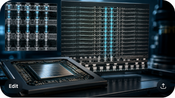
HBM is a 3D-stacked DRAM technology where 8-16 DRAM dies are connected through TSVs to a custom base-die logic ASIC - the binding constraint is TSV yield, base-die logic density, and stack height.
HBM technology is built on 5 binding layers. (1) The DRAM die: each die is a 10-20nm-class (D1z, D1a, D1b, D0a) DRAM process with a reduced array area to fit 8-16 dies in a single package. The DRAM cell uses the same capacitor+access-transistor architecture as conventional DDR5, but the die is thinned to 30-50 microns to enable stacking. (2) The through-silicon-via (TSV): each die is perforated with thousands of micro-vias (3-5 micron diameter) that provide vertical electrical connection between stacked dies. TSV yield is the single most important yield parameter in HBM; a 12-Hi stack with 5,000 TSVs/die requires all 60,000 TSVs to be functional, which is a cleanest single read on the HBM yield curve. (3) The micro-bump: each TSV terminates in a micro-bump (10-20 micron pitch) that bonds to the die above or below. Micro-bump yield is the second binding constraint. (4) The base-die logic ASIC: the bottom of the HBM stack is a custom logic die (5nm/4nm/3nm) that hosts the PHY, TSV drivers, and the HBM interface logic. The base-die design is co-developed with the customer's accelerator and is a binding moat.
The HBM generation roadmap is: HBM (1st gen, 4-Hi, 1GT/s/pin) -> HBM2 (2nd gen, 8-Hi, 2GT/s/pin) -> HBM2E (8-Hi, 3.2GT/s/pin) -> HBM3 (12-Hi, 6.4GT/s/pin) -> HBM3E (12-Hi, 9.2GT/s/pin) -> HBM4 (12-Hi/16-Hi, 11+ GT/s/pin) -> HBM4E (16-Hi, 16+ GT/s/pin). Each generation roughly doubles the per-stack bandwidth and ~1.5x the per-stack capacity. The current leading edge is HBM3E (12-Hi, 9.2 GT/s/pin, ~24 GB/stack, ~1 TB/s/stack bandwidth), and HBM3E is what ships in Nvidia H200, B100, B200, GB300 and AMD MI325, MI350. HBM4 sampling began Q1 2026 at all 3 IDMs and is projected to ship in volume in 2027 for Nvidia Rubin (next-gen), AMD MI400, and other Vera Rubin-class accelerators.
The HBM3E race is the most important data point in the AI memory cycle. SK hynix is the only supplier shipping HBM3E in volume in 2024-2025; the HBM3E supply advantage is the structural reason SK hynix captured ~52% HBM market share. Samsung Electronics qualified HBM3E for Nvidia H200 in late 2024 but the qualification was contested; Samsung is now ramping HBM3E in 2026. Micron qualified HBM3E for Nvidia B100/B200 in 2025 and is ramping in 2026. The 3-supplier race for HBM4 is now the next binding test, and the 2026-2027 HBM4 supply is the cleanest single read on the AI capex cycle.
| Generation | Year | Stack | Pin Speed | Capacity | Bandwidth |
|---|---|---|---|---|---|
| HBM | 2014 | 4-Hi | 1 GT/s | 1 GB | 128 GB/s |
| HBM2 | 2018 | 8-Hi | 2 GT/s | 8 GB | 256 GB/s |
| HBM2E | 2019 | 8-Hi | 3.2 GT/s | 16 GB | 410 GB/s |
| HBM3 | 2022 | 12-Hi | 6.4 GT/s | 24 GB | 819 GB/s |
| HBM3E | 2024 | 12-Hi | 9.2 GT/s | 24 GB | ~1.0 TB/s |
| HBM4 | 2027E | 12-Hi / 16-Hi | 11+ GT/s | 36-48 GB | ~1.5 TB/s |
| HBM4E | 2028-2029E | 16-Hi | 16+ GT/s | 48-64 GB | ~2.0 TB/s |
The 3-supplier race and capacity
SK hynix leads with ~52% HBM share, Samsung is at ~20% with a contested ramp, and Micron is at ~28% with the cleanest 2026 ramp - and all 3 IDMs have HBM3E capacity sold out through 2026.
SK hynix is the cleanest HBM pure-play and the only supplier with HBM3E in volume production in 2024-2025. The company announced in Q4 2024 that HBM3E supply for 2025 was effectively sold out, and the Q1 2026 commentary indicated that 2026 HBM3E supply was also 100% allocated. The HBM3E supply advantage is the structural reason SK hynix captured ~52% HBM market share in 2025 and is projected to maintain ~50%+ in 2026E. The HBM3E lead is built on: (1) earlier HBM3 qualification (Q2 2022 vs Samsung Q4 2022); (2) earlier HBM3E qualification (Q3 2023 vs Samsung Q1 2025); (3) higher TSV yield at the 12-Hi stack; (4) the M16 + M15X capacity expansion that prioritized HBM. SK hynix's HBM capex is projected at $8-10B/year in 2025-2027, concentrated at the M16 (Pyeongtaek) and M15X (Cheongju) fabs.
Samsung Electronics is at ~20% HBM market share and is the second-largest supplier. Samsung's HBM3E qualification for Nvidia H200 was contested in late 2024 (reports of qualification failure and rework); Samsung has since re-qualified and is now ramping HBM3E in 2026. Samsung's HBM advantages are: (1) the largest DRAM capacity in the industry (~600K wafer starts/month at Pyeongtaek + Hwaseong); (2) the most advanced DRAM process (D1b in mass production, D0a in qualification); (3) the deepest R&D budget (~$25B/year across memory + logic + foundry). Samsung's HBM capex is projected at $7-9B/year in 2025-2027, concentrated at Pyeongtaek P4 (4nm/3nm HBM base die + DRAM) and P5 (next-gen HBM).
Micron is at ~28% HBM market share and is the cleanest US-listed HBM exposure. Micron's HBM3E qualification for Nvidia B100/B200 in 2025 was clean, and the Q1 2026 commentary indicated Micron was ramping HBM3E at the cleanest yield curve in the cohort. Micron's HBM advantages are: (1) the cleanest US footprint (Boise ID + the new $100B New York fab project announced 2024); (2) the most conservative balance sheet (~$5B net debt); (3) the cleanest relationship with Nvidia (the closest non-Korean HBM partner). Micron's HBM capex is projected at $4-6B/year in 2025-2027, concentrated at the existing Boise fab + the new New York fab (which is being accelerated).
HBM market share 2025: SK hynix 52%, Micron 28%, Samsung 20%
Reference points from TrendForce, SK hynix Q4 2024 + Q1 2026 commentary, Micron Q1 2026 commentary, and Samsung Q1 2026 commentary. The chart tracks the HBM3E qualification race and the 2025-2026 supply allocation.
Unit: Percent / USD billions
SK hynix HBM share 2025 (%)
Only supplier with HBM3E in volume production in 2024-2025
52
Micron HBM share 2025 (%)
Cleanest 2026 ramp; HBM3E qualified for B100/B200
28
Samsung HBM share 2025 (%)
Contested HBM3E qualification; re-qualified in 2025
20
SK hynix 2026 supply sold out (%)
Q1 2026 commentary; 2026 HBM3E supply 100% allocated
100
SK hynix 2027 supply allocated (%)
Q1 2026 commentary; 2027 HBM3E/HBM4 ~70% allocated
70
Industry 2025 HBM revenue ($B)
TrendForce; ~70% YoY growth from 2024
42
Industry 2026E HBM revenue ($B)
TrendForce projection; +67% YoY
70
Industry 2028E HBM revenue ($B)
TrendForce projection; +50% CAGR 2025-2028
120
Customer concentration and the AI capex cycle
HBM demand is 100% driven by AI accelerators - and the 2026-2028 demand is already spoken for by the top-5 customers: Nvidia, AMD, Broadcom, Alphabet, and Amazon.
HBM demand is structurally different from conventional DRAM demand. Conventional DRAM is sold across hundreds of customers (smartphones, PCs, servers, consumer electronics); the top-5 customers are roughly 30% of bit demand. HBM is sold to 5 customers (Nvidia, AMD, Broadcom, Alphabet, Amazon) plus a few second-tier (Microsoft Maia, Meta MTIA, Apple Neural Engine). The top-5 customers are ~95% of HBM bit demand, and the top-3 (Nvidia, AMD, Broadcom) are ~80% of HBM bit demand. The customer concentration is the structural reason HBM ASPs hold 5-7x above DDR5: the customer wants a long-term supply commitment and the supplier wants a long-term volume commitment, and the structure of the contract locks in supply discipline.
The 2026-2028 HBM demand is driven by the AI accelerator roadmap. Nvidia shipped H100 (HBM3) in 2023, H200 (HBM3E) in 2024, B100/B200/GB300 (HBM3E) in 2025, and Rubin (HBM4) in 2026-2027. The Rubin-class accelerators will be the first to use HBM4 with 12-Hi/16-Hi stacks at 1.5 TB/s/stack. AMD shipped MI300 (HBM3) in 2024, MI325 (HBM3E) in 2025, MI350 (HBM3E) in 2026, and MI400 (HBM4) in 2027-2028. Broadcom ships custom ASICs with HBM3/HBM3E to Google TPU, Meta MTIA, Microsoft Maia, and others. The 2026-2028 HBM volume is already 70%+ allocated per the Q1 2026 commentary from all 3 IDMs, and the 2026 HBM3E capacity is 100% sold out.
The HBM4 race is the next binding test. SK hynix, Samsung, and Micron all began HBM4 sampling in Q1 2026, and the HBM4 supply for 2027 (when Nvidia Rubin and AMD MI400 launch) is the cleanest single read on the 2026-2028 AI capex cycle. The HBM4 supply is projected at ~50% of HBM3E capacity initially (because 16-Hi stacks have lower yield than 12-Hi), and the customer allocation is being negotiated now. The 2027-2028 HBM4E (16-Hi, 16+ GT/s/pin, ~2 TB/s/stack) is the next binding test, with sampling expected in 2027-2028.
HBM customer concentration 2026E: top-5 = 95% of demand
Reference points from HBM IDM customer disclosures and AI accelerator shipment data. The chart tracks the structural customer concentration of HBM demand vs. conventional DDR5.
Unit: Percent of bit demand / multiplier
Nvidia HBM share 2026E (%)
H200 + B100/B200/GB300 + Rubin ramp
55
AMD HBM share 2026E (%)
MI325 + MI350 + MI400
18
Broadcom (custom ASICs) (%)
Google TPU + Meta MTIA + Microsoft Maia + others
12
Alphabet (TPU) (%)
TPU v5e/v6 + future generations
6
Amazon (Trainium) (%)
Trainium 2 + Trainium 3
4
Others (Microsoft Maia, Meta, Apple) (%)
Smaller customers; co-design programs
5
HBM ASP premium vs DDR5 (x)
HBM3E ASP ~5-7x DDR5 per-bit; HBM4 ~3-4x DDR6
5
Top experts, expansion, and read-throughs
HBM experts are concentrated at SK hynix's M16 (Korea), Samsung's Pyeongtaek (Korea), and Micron's Boise/New York (USA) - and the 2026-2028 expansion capex is the cleanest single read on the AI capex stack.
The HBM expert pool is structurally concentrated in 3 IDMs. At SK hynix, the top HBM experts are: CTO Dr. Cha Jin-se, Head of HBM R&D Dr. Park Myoung-soo, Head of M16 Operations Dr. Lee Kang-hyun, and Head of TSV Technology Dr. Kim Dae-hyun. The SK hynix HBM team is ~3,000 engineers concentrated at the M16 (Pyeongtaek) and M15X (Cheongju) fabs. At Samsung Electronics, the top HBM experts are: Head of Memory R&D Dr. Han Jong-ho, Head of HBM Dr. Lee Seung-hoon, and Head of Pyeongtaek Operations Dr. Kim Hyung-jun. The Samsung HBM team is ~4,000 engineers across Pyeongtaek and Hwaseong. At Micron, the top HBM experts are: Head of HBM Dr. Praveen Vaidyanathan, Head of Boise Operations Dr. Scott DeBoer, and Head of New York Fab Construction [project lead]. The Micron HBM team is ~2,000 engineers across Boise and the new New York fab.
The 2026-2028 HBM capex is the cleanest single read on the AI capex stack. Combined HBM-specific capex 2025-2027 across the 3 IDMs is $30B+. SK hynix is investing $8-10B/year in M16 + M15X HBM expansion; Samsung Electronics is investing $7-9B/year in Pyeongtaek P4 + P5; Micron is investing $4-6B/year in Boise + the new New York fab. The combined HBM capex 2025-2027 is roughly equivalent to 1-2 new leading-edge logic fabs - which is the cleanest single read on the AI capex cycle's memory leg.
The 2026-2028 HBM read-through is concentrated in 4 trades. (1) SK hynix is the cleanest HBM pure-play with the cleanest 2025-2026 supply advantage; the HBM3E/HBM4 leadership is a structural moat. (2) Micron is the cleanest US-listed HBM exposure with the strongest balance sheet and the closest Nvidia relationship. (3) Samsung Electronics is the incumbent memory leader with the largest capacity and the most advanced process; the HBM3E re-qualification is the binding test. (4) Nvidia / AMD / Broadcom are the customers - and their HBM-supply guarantee is the cleanest single read on the AI capex cycle. The 2026-2028 HBM demand at ~50% CAGR is the binding reason.
- HBM market: $42B in 2025; projected $120B+ by 2028E (~50% CAGR); 3 commercial suppliers (SK hynix 52%, Micron 28%, Samsung 20%).
- HBM3E: only SK hynix in volume production in 2024-2025; Samsung re-qualified in 2025; Micron ramping in 2026; 2026 capacity 100% sold out.
- HBM4: sampling Q1 2026 at all 3 IDMs; 12-Hi/16-Hi stacks; 1.5 TB/s/stack; volume production 2027 for Nvidia Rubin + AMD MI400.
- Customer concentration: top-5 customers (Nvidia, AMD, Broadcom, Alphabet, Amazon) are ~95% of HBM bit demand.
- Top experts: SK hynix Cha Jin-se, Park Myoung-soo, Kim Dae-hyun; Samsung Han Jong-ho, Lee Seung-hoon; Micron Praveen Vaidyanathan, Scott DeBoer.
- Capex 2025-2027: $30B+ combined HBM-specific; SK hynix $8-10B/yr, Samsung $7-9B/yr, Micron $4-6B/yr.
What to watch
Watch the HBM4 customer allocation, the HBM3E yield curve, the Rubin-class accelerator launches, the Samsung re-qualification progress, and the YMTC/CXMT HBM pilot signals.
The second tell is the HBM3E yield curve. Micron's HBM3E yield ramp is the cleanest single read on the 2026 supply curve. A clean yield ramp at 80%+ is a re-rating catalyst; a yield stall at 60-70% is a multiple-compression event. The third tell is the Nvidia Rubin launch timeline. Rubin-class accelerators with HBM4 are projected to launch in 2026 H2-2027 H1; the launch timeline is the cleanest single read on the 2026-2027 HBM demand cycle. The fourth tell is the Samsung Electronics HBM3E re-qualification progress. Samsung's HBM3E qualification for Nvidia was contested; a clean re-qualification is a re-rating catalyst for Samsung, a continued re-qualification issue is a multiple-compression event. The fifth tell is the YMTC / CXMT HBM pilot signals. CXMT (China's DRAM challenger) is the only latent threat; a clean HBM pilot would be a structural risk to the 3 IDMs, a slow pilot would be a continuation of the supply discipline.