%22%2F%3E%0A%20%20%3Ccircle%20cx%3D%22220%22%20cy%3D%22150%22%20r%3D%22180%22%20fill%3D%22%2322d3ee%22%20fill-opacity%3D%220.12%22%2F%3E%0A%20%20%3Ccircle%20cx%3D%221010%22%20cy%3D%22130%22%20r%3D%22220%22%20fill%3D%22%2338bdf8%22%20fill-opacity%3D%220.08%22%2F%3E%0A%20%20%3Ccircle%20cx%3D%22920%22%20cy%3D%22520%22%20r%3D%22170%22%20fill%3D%22%2322d3ee%22%20fill-opacity%3D%220.06%22%2F%3E%0A%20%20%3Cpath%20d%3D%22M140%20430h920%22%20stroke%3D%22url(%23line)%22%20stroke-width%3D%2212%22%20stroke-linecap%3D%22round%22%2F%3E%0A%20%20%3Cpath%20d%3D%22M220%20360c120-150%20260-220%20380-220s260%2070%20380%20220%22%20fill%3D%22none%22%20stroke%3D%22%2367e8f9%22%20stroke-opacity%3D%220.5%22%20stroke-width%3D%2216%22%20stroke-linecap%3D%22round%22%20stroke-linejoin%3D%22round%22%2F%3E%0A%20%20%3Cpath%20d%3D%22M300%20398h600%22%20stroke%3D%22%2394a3b8%22%20stroke-opacity%3D%220.24%22%20stroke-width%3D%228%22%20stroke-linecap%3D%22round%22%2F%3E%0A%20%20%3Ctext%20x%3D%22220%22%20y%3D%22510%22%20fill%3D%22%23e2e8f0%22%20fill-opacity%3D%220.7%22%20font-family%3D%22Arial%2C%20Helvetica%2C%20sans-serif%22%20font-size%3D%2238%22%20letter-spacing%3D%228%22%3EINSIGHTS%3C%2Ftext%3E%0A%3C%2Fsvg%3E)
Bottom line
The moat moved from the wafer to the package.
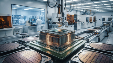
AI chips are no longer just about transistor count or process node. The real system is now a stack: compute dies, HBM, interconnect, substrates, thermal management, and test. The companies that can integrate those pieces with high yield and fast time-to-volume are pulling away.
That means advanced packaging is not a niche post-processing step. It is the place where value, scarcity, and scheduling power are increasingly concentrated.
What changed
TSMC is scaling packaging like a first-class technology platform.
CoWoS and 3D roadmap
The chart uses the published packaging roadmap from TSMC's 2026 North America Technology Symposium. It captures the move from today's 5.5-reticle CoWoS to the planned 14-reticle and 40-reticle system scales.
Unit: reticles
CoWoS now
Current production
5.5
CoWoS 2028
Planned production
14
SoW-X 2029
Planned system-on-wafer
40
| Platform | Published detail | Why it matters |
|---|---|---|
| 3DFabric | TSMC says it includes SoIC, CoWoS, and InFO. | Packaging is now a first-class system-integration stack, not an afterthought. |
| CoWoS today | TSMC is producing 5.5-reticle size CoWoS. | This reflects how large AI packages have already become. |
| CoWoS 2028 | 14-reticle CoWoS can integrate about 10 large compute dies and 20 HBM stacks. | That is a massive jump in integration complexity. |
| SoIC 2029 | A14-to-A14 SoIC is scheduled for production in 2029. | 3D stacking is moving deeper into the mainstream AI roadmap. |
| COUPE 2026 | TSMC says co-packaged optics on substrate begins production in 2026 with 2x power efficiency and 10x latency reduction vs pluggables. | Power and latency become package-level design problems. |
Why GPU specs matter
The package has to keep up with the chip.
NVIDIA's Blackwell architecture packs 208 billion transistors, uses two reticle-limited dies connected by a 10 TB/s chip-to-chip interconnect, and is being positioned as the engine behind AI factories. AMD's MI350 series pushes 288GB of HBM3E and 8TB/s bandwidth. Those are not just product specs; they are packaging requirements.
| Vendor / platform | Published spec | Implication for packaging |
|---|---|---|
| NVIDIA Blackwell | 208B transistors and 10 TB/s chip-to-chip interconnect | The chip is already a system-level assembly problem. |
| NVIDIA GB200 NVL72 | 72-GPU rack-scale design | Scale-out demand pushes packaging, networking, and cooling together. |
| AMD MI350 | 288GB HBM3E and 8TB/s bandwidth | Memory density and bandwidth are now the product. |
| AMD MI355X | Same 288GB HBM3E / 8TB/s class with higher-density AI infrastructure focus | The market is optimizing around high-density inference and training platforms. |
- The more memory stacks a package must carry, the more the package becomes the product.
- The more die-to-die bandwidth matters, the more substrate, thermal, and yield constraints show up in the P&L.
- The engineering challenge is no longer only lithography. It is coordination across the whole supply chain.
Why ASE matters
The rest of the ecosystem is building capacity behind TSMC.
ASE and WUS said in May 2026 that they will build an advanced AI packaging hub in Kaohsiung. The companies said the facility will create more than 2,000 jobs, cover more than 113,000 square meters, and complete by September 2029. ASE also said in March 2026 that it was breaking ground on a new high-tech facility with NT$17.8 billion of investment and an expected completion date in the second quarter of 2028.
| Company / project | Published detail | Interpretation |
|---|---|---|
| ASE + WUS hub | More than 2,000 jobs; >113,000 square meters; completion by Sep. 2029. | Advanced packaging is scaling into an industrial cluster, not a single factory. |
| ASE Kaohsiung facility | NT$17.8B investment and completion target in Q2 2028. | Capacity is being added because demand is still outrunning supply. |
| Power infrastructure | ASE says the site will include a 161kV substation. | Even packaging now needs energy planning. |
Investor read-through
Packaging is becoming its own profit pool.
- TSMC wins when customers need a tightly integrated 3DFabric stack and are willing to pay for time-to-volume.
- ASE benefits when the market needs more packaging, test, and system-integration capacity than the fabs alone can absorb.
- NVIDIA and AMD benefit when better packaging lets them ship higher-performance systems, but they also depend on the ecosystem not becoming a constraint.
- Substrates, materials, thermal solutions, and test equipment all become more important when packages get larger and denser.
| Bottleneck | What to watch | Why it matters |
|---|---|---|
| Substrates | Lead times and pricing | Large packages need more advanced substrates and better yield. |
| HBM | Stack availability and integration | Memory density must arrive on schedule or the package is stranded. |
| Power and cooling | Thermal design and substation capacity | Denser packages generate more heat and need more infrastructure. |
| Test and reliability | Yield and failure rates | Integration complexity can destroy margins if the test stack is weak. |