
%22%2F%3E%0A%20%20%3Ccircle%20cx%3D%22220%22%20cy%3D%22150%22%20r%3D%22180%22%20fill%3D%22%2322d3ee%22%20fill-opacity%3D%220.12%22%2F%3E%0A%20%20%3Ccircle%20cx%3D%221010%22%20cy%3D%22130%22%20r%3D%22220%22%20fill%3D%22%2338bdf8%22%20fill-opacity%3D%220.08%22%2F%3E%0A%20%20%3Ccircle%20cx%3D%22920%22%20cy%3D%22520%22%20r%3D%22170%22%20fill%3D%22%2322d3ee%22%20fill-opacity%3D%220.06%22%2F%3E%0A%20%20%3Cpath%20d%3D%22M140%20430h920%22%20stroke%3D%22url(%23line)%22%20stroke-width%3D%2212%22%20stroke-linecap%3D%22round%22%2F%3E%0A%20%20%3Cpath%20d%3D%22M220%20360c120-150%20260-220%20380-220s260%2070%20380%20220%22%20fill%3D%22none%22%20stroke%3D%22%2367e8f9%22%20stroke-opacity%3D%220.5%22%20stroke-width%3D%2216%22%20stroke-linecap%3D%22round%22%20stroke-linejoin%3D%22round%22%2F%3E%0A%20%20%3Cpath%20d%3D%22M300%20398h600%22%20stroke%3D%22%2394a3b8%22%20stroke-opacity%3D%220.24%22%20stroke-width%3D%228%22%20stroke-linecap%3D%22round%22%2F%3E%0A%20%20%3Ctext%20x%3D%22220%22%20y%3D%22510%22%20fill%3D%22%23e2e8f0%22%20fill-opacity%3D%220.7%22%20font-family%3D%22Arial%2C%20Helvetica%2C%20sans-serif%22%20font-size%3D%2238%22%20letter-spacing%3D%228%22%3EINSIGHTS%3C%2Ftext%3E%0A%3C%2Fsvg%3E)
Industry structure
ALD is a 4-player equipment oligopoly - Applied Materials ~50%, Lam Research ~20%, Tokyo Electron ~15%, ASM International ~10% - and the 2026-2028 ALD demand is the cleanest single read on the leading-edge AI capex stack.
Atomic Layer Deposition (ALD) is the most concentrated thin-film equipment oligopoly in the semiconductor industry, and the 2026-2028 ALD demand is the cleanest single read on the leading-edge AI capex stack. The 4 leading-edge ALD suppliers are: Applied Materials (AMAT) with about 50 percent global share, Lam Research (LRCX) with 20 percent, Tokyo Electron (8035.T) with 15 percent, and ASM International (ASM.AS) with 10 percent (with the strongest position in the thermal ALD sub-segment). The 2025 ALD equipment market is about $8B, projected to grow to about $15B by 2028E at 25 percent CAGR, driven by the GAA (gate-all-around) + HBM + 3D NAND leading-edge demand. The customer base is concentrated in 4 IDMs: TSMC (TSM) (about 50 percent of ALD demand), Samsung Electronics (005930.KS) (20 percent), Intel (INTC) (15 percent), and SK hynix (000660.KS) (10 percent).
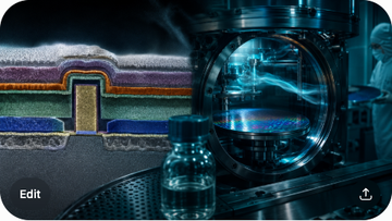
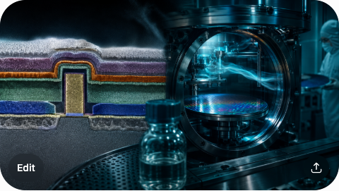
ALD is a thin-film deposition technology that builds atomic-scale films one layer at a time, using sequential self-limiting surface reactions. The binding advantage of ALD over conventional CVD (chemical vapor deposition) is the atomic-scale thickness control and the conformality on high-aspect-ratio structures (3D NAND holes, HBM TSVs, GAA nanosheet channels). The ALD technology taxonomy is: thermal ALD (uses thermal energy to drive the surface reaction, cleanest sub-nm thickness control), plasma-enhanced ALD or PEALD (uses plasma to drive the surface reaction at lower temperatures, binding for temperature-sensitive films), and spatial ALD (uses separated precursor + co-reactant zones, cleanest for high-throughput batch ALD on 3D NAND). The 3 sub-segments are dominated by different suppliers: ASM International leads thermal ALD, Applied Materials leads PEALD, Lam Research leads spatial ALD for 3D NAND.
The 2025-2026 ALD demand is driven by the GAA + HBM + 3D NAND leading-edge roadmap. The 3nm logic chip needs 50+ ALD layers (vs 25 at 7nm), the HBM3E 12-Hi stack needs 30+ ALD layers per stack, the HBM4E 16-Hi stack needs 40+ ALD layers per stack, and the 400L+ 3D NAND needs 20+ ALD layers per die. The ALD layer count is the cleanest single read on the AI capex cycle's thin-film leg, and the 2026-2028 ALD capex is the cleanest single read on the AI capex stack.
The ALD technology stack
ALD is built on 5 binding layers: the precursor (TMA, HfCl4, TiCl4), the co-reactant (H2O, O3, NH3, H2), the reactor (single-wafer or batch), the plasma source (for PEALD), and the in-situ metrology - each is a 10+ year R&D moat.
ALD technology is built on 5 binding layers. (1) The precursor: the ALD precursor is a volatile metal-organic or metal-halide compound that reacts with the substrate surface in a self-limiting manner. The most common ALD precursors are TMA (trimethylaluminum for Al2O3 ALD), HfCl4 (hafnium tetrachloride for HfO2 high-k ALD), TiCl4 (titanium tetrachloride for TiO2 or TiN ALD), TEMA (tetrakis-ethylmethylamino-hafnium for HfO2 PEALD), and TDMAH (tetrakis-dimethylamino-hafnium for HfO2 thermal ALD). The precursor chemistry is the binding sensitivity lever; a 2x improvement in precursor reactivity enables a 2x reduction in ALD cycle time. The precursor supply is dominated by about 5 specialty chemical companies: Air Products (APD), Linde (LIN), and a few Korean challengers like UP Chemical (078910.KS). (2) The co-reactant: the ALD co-reactant is the second precursor that completes the surface reaction. The most common co-reactants are H2O (for oxide ALD), O3 (for higher-quality oxide ALD), NH3 (for nitride ALD), and H2 (for metal ALD). The co-reactant chemistry is the binding quality lever.
(3) The reactor: the ALD reactor is the chamber that hosts the ALD surface reaction. The single-wafer ALD reactor (used for logic + HBM) processes 1 wafer at a time, with the wafer on a heated stage (200-400C) and the precursors + co-reactants pulsed in alternating sequences. The batch ALD reactor (used for 3D NAND) processes 50-100 wafers at a time. The single-wafer ALD reactor ASP is 5-8M USD, and the batch ALD reactor ASP is 3-5M USD per chamber. (4) The plasma source: the PEALD reactor adds a plasma source (typically an inductively coupled plasma, ICP) that enables the ALD reaction at lower temperatures (down to 50-100C vs 200-400C for thermal ALD). The plasma source is the binding temperature lever. (5) The in-situ metrology: the ALD reactor has in-situ metrology (ellipsometry, reflectometry, or spectroscopic ellipsometry) that measures the film thickness in real time. The in-situ metrology is the binding yield lever.
The 4-supplier ALD oligopoly
Applied Materials leads with ~50% share (strong in PEALD), Lam Research is at ~20% (strong in spatial ALD for 3D NAND), Tokyo Electron is at ~15% (strong in batch ALD), and ASM International is at ~10% (strongest in thermal ALD).
Applied Materials (AMAT) is the largest ALD supplier with about 50 percent global share, dominated by the Producer Selectra and Olympia ALD product lines. Applied Materials ALD advantages are: the broadest ALD product portfolio (thermal ALD, PEALD, batch ALD); the strongest PEALD market position (the binding for low-temperature films at GAA + backside power); the largest R&D budget (about $3B/year in ALD + CVD + PVD); and the deepest customer relationships (especially with TSMC and Samsung). Applied Materials ALD revenue is about 3-4B USD per year in 2025-2027, with the ALD business growing at 20-25 percent CAGR. The ALD business is concentrated at the Santa Clara + Austin R&D centers, with about 2000 ALD engineers globally.
Lam Research (LRCX) is the second-largest ALD supplier with about 20 percent global share, dominated by the Striker and VECTOR ALD product lines. Lam Research ALD advantages are: the strongest spatial ALD position (the binding for 3D NAND high-aspect-ratio ALD); the deepest relationship with SK hynix and Samsung on memory ALD; the cleanest batch ALD reactor for 400L+ 3D NAND. Lam Research ALD revenue is about 1.5-2B USD per year in 2025-2027, with the ALD business growing at 25 percent CAGR. The ALD business is concentrated at the Fremont + Tualatin R&D centers, with about 1000 ALD engineers globally.
Tokyo Electron (8035.T) is the third-largest ALD supplier with about 15 percent global share, dominated by the Triase+ and LX-1 ALD product lines. Tokyo Electron ALD advantages are: the strongest batch ALD position (the binding for high-throughput ALD); the cleanest Japan-customer relationship (Kioxia, Sony, Renesas); the cleanest low-temperature PEALD for 3D NAND. Tokyo Electron ALD revenue is about 1-1.5B USD per year in 2025-2027, with the ALD business growing at 20 percent CAGR. ASM International (ASM.AS) is the fourth-largest ALD supplier with about 10 percent global share, with the strongest position in thermal ALD (the binding for HKMG + high-k logic films). ASM ALD revenue is about 0.8-1B USD per year in 2025-2027, with the ALD business growing at 30 percent CAGR (the fastest in the cohort).
ALD supplier share 2025-2026E: Applied Materials 50%, Lam Research 20%, Tokyo Electron 15%, ASM International 10%
Reference points from SEMI market data and the 4 ALD suppliers investor disclosures. The chart tracks the ALD supplier share split and the 2025 vs 2026E ALD revenue per supplier.
Unidad: USD millions
Applied Materials 2025 ($M)
~50% share; PEALD + thermal ALD + batch ALD
3,500
Lam Research 2025 ($M)
~20% share; spatial ALD + batch ALD
1,400
Tokyo Electron 2025 ($M)
~15% share; batch ALD + PEALD
1,050
ASM International 2025 ($M)
~10% share; thermal ALD leader
700
Applied Materials 2026E ($M)
+20% YoY; GAA + backside power ramp
4,200
Lam Research 2026E ($M)
+25% YoY; 3D NAND + memory
1,750
Tokyo Electron 2026E ($M)
+19% YoY; batch ALD + Japan customer
1,250
ASM International 2026E ($M)
+30% YoY; thermal ALD leader; fastest grower
910
ALD demand and the AI capex cycle
The 2026-2028 ALD demand is driven by GAA + HBM + 3D NAND - and the customer base is TSMC (~50%) + Samsung (~20%) + Intel (~15%) + SK hynix (~10%) = ~95% of demand.
The 2026-2028 ALD demand is the cleanest single read on the leading-edge AI capex cycle. The demand is driven by the GAA + backside power roadmap at TSMC (2nm in 2025-2026, 1.4nm in 2026-2027, 1nm in 2028) and Samsung (2nm in 2025-2026) and Intel (18A in 2025-2026, 14A in 2026-2027). The HBM roadmap at SK hynix (HBM3E 12-Hi in 2024-2025, HBM4 12-Hi/16-Hi in 2026-2027, HBM4E 16-Hi in 2027-2028) and Samsung (HBM3E 12-Hi in 2025, HBM4 in 2026-2027) drives additional ALD demand. The 3D NAND roadmap at Samsung V9 290L in 2025, V10 430L in 2026-2027, SK hynix V9 238L in 2025, V10 321L in 2026, Kioxia BiCS Gen 8 290L in 2025-2026, Micron G9 232L in 2025, G10 in 2026-2027, and Sandisk BiCS Gen 8 290L in 2025-2026 is the third leg. The combined GAA + HBM + 3D NAND roadmap is the binding reason ALD demand grows at 25 percent CAGR in 2025-2028.
The customer base is structurally concentrated in 4 IDMs: TSMC (50 percent of ALD demand, the cleanest single exposure to the GAA + backside power roadmap), Samsung Electronics (20 percent, exposed to GAA + HBM + 3D NAND), Intel (15 percent, exposed to 18A + 14A + EMIB), and SK hynix (10 percent, exposed to HBM + 3D NAND). The top-4 customers are about 95 percent of ALD demand, and the customer concentration is the structural reason the 2026-2028 ALD capacity is 100 percent allocated.
The 2026-2028 ALD capex is the cleanest single read on the AI capex cycle thin-film leg. The combined ALD-specific capex 2025-2027 across the 4 IDM customers is 20B+ USD (TSMC 8B, Samsung 5B, Intel 4B, SK hynix 3B). The capex is concentrated at the GAA + backside power + HBM + 3D NAND ramp, and the 2027-2028 ALD capex is the binding reason. The ALD capex is roughly 5-8 percent of the total wafer fab equipment (WFE) capex, which is the cleanest single read on the thin-film share of the WFE pie.
Top experts, expansion, and read-throughs
ALD experts are concentrated at 4 hubs (Applied Materials Santa Clara, Lam Research Fremont, Tokyo Electron Tokyo, ASM International Almere) - and the 2026-2028 ALD capex is the cleanest single read on the AI capex cycle thin-film leg.
The ALD expert pool is structurally concentrated in 4 hubs. At Applied Materials (AMAT), the top ALD experts are Group VP of ALD Dr. Prabu Raja, VP of ALD Engineering Dr. Srinivas Gandikota, and VP of PEALD Dr. Ming Li. The Applied Materials ALD team is about 2000 engineers at Santa Clara + Austin. At Lam Research (LRCX), the top ALD experts are Group VP of ALD Dr. Dave Hemker, VP of Spatial ALD Dr. Richard Gottscho, and VP of Batch ALD Dr. Reza Arghavani. The Lam Research ALD team is about 1000 engineers at Fremont + Tualatin. At Tokyo Electron (8035.T), the top ALD experts are Senior VP of ALD Dr. Tetsuro Higashi, VP of Batch ALD Dr. Masayuki Tomoyasu, and Head of Low-Temp PEALD Dr. Yoshihiro Koga. The Tokyo Electron ALD team is about 1000 engineers at Tokyo + Hosaka. At ASM International (ASM.AS), the top ALD experts are CTO Dr. Hichem M Saad, VP of Thermal ALD Dr. Ruud Schropp, and VP of PEALD Dr. Wilhelmus Kessels. The ASM International ALD team is about 600 engineers at Almere (Netherlands) + Phoenix.
The 2026-2028 ALD read-through is concentrated in 4 trades. (1) Applied Materials (AMAT) is the largest ALD supplier with 50 percent share; the cleanest single exposure to the GAA + backside power + HBM + 3D NAND ramp. (2) Lam Research (LRCX) is the second-largest ALD supplier with 20 percent share; the cleanest exposure to 3D NAND + memory. (3) ASM International (ASM.AS) is the fourth-largest ALD supplier with 10 percent share but the fastest-growing at 30 percent CAGR; the cleanest exposure to thermal ALD logic. (4) Tokyo Electron (8035.T) is the third-largest ALD supplier with 15 percent share; the cleanest exposure to batch ALD + Japan-customer. The 2026-2028 ALD demand at 25 percent CAGR is the cleanest single read on the AI capex cycle thin-film leg.
- ALD equipment market: about $8B in 2025; projected about $15B by 2028E at 25 percent CAGR; 4-supplier oligopoly (AMAT 50%, LRCX 20%, TEL 15%, ASMI 10%).
- ALD layer count: 3nm logic = 50+ layers; 2nm logic = 60+ layers; HBM3E 12-Hi = 30+ layers; HBM4E 16-Hi = 40+ layers; 400L+ 3D NAND = 20+ layers.
- ALD reactor ASP: 5-8M USD single-wafer; 3-5M USD batch (3D NAND); PEALD adds 20% premium over thermal ALD.
- Customer concentration: TSMC 50% + Samsung 20% + Intel 15% + SK hynix 10% = 95% of demand.
- Capex 2025-2027: 20B+ USD combined; TSMC $8B, Samsung $5B, Intel $4B, SK hynix $3B.
- Top experts: AMAT Prabu Raja, Srinivas Gandikota, Ming Li; LRCX Dave Hemker, Richard Gottscho, Reza Arghavani; TEL Tetsuro Higashi, Masayuki Tomoyasu, Yoshihiro Koga; ASMI Hichem M Saad, Ruud Schropp, Wilhelmus Kessels.
- Read-through: Applied Materials (AMAT) cleanest exposure; Lam Research (LRCX) 3D NAND + memory; ASM International (ASM.AS) fastest-growing; Tokyo Electron (8035.T) batch ALD + Japan.
What to watch
Watch the GAA + backside power ALD ramp, the HBM4 + HBM4E ALD layer count, the 400L+ 3D NAND ALD demand, the ASM International thermal ALD share, and the Applied Materials PEALD market position.
The first tell is the GAA + backside power ALD ramp. The 2nm logic + backside power roadmap at TSMC, Samsung, and Intel is the cleanest single demand driver for ALD. A clean 2nm ramp in 2026 is a re-rating catalyst for Applied Materials (AMAT) and ASM International (ASM.AS); a 2nm ramp delay is a multiple-compression event. Watch the quarterly IDM capex disclosures as the cleanest read on the ALD cycle.
The second tell is the HBM4 + HBM4E ALD layer count. HBM4E 16-Hi needs 40 ALD layers per stack, which is the cleanest single read on the HBM ALD demand. A clean HBM4E sampling in 2027 is a re-rating catalyst; a HBM4E delay is a multiple-compression event. The third tell is the 400L+ 3D NAND ALD demand. The 400L+ 3D NAND roadmap at Samsung, SK hynix, Kioxia, and Micron needs 20 ALD layers per die, which is the cleanest single read on the 3D NAND ALD demand. A clean 400L+ ramp in 2027 is a re-rating catalyst for Lam Research (LRCX) and Tokyo Electron (8035.T). The fourth tell is the ASM International (ASM.AS) thermal ALD share. ASM thermal ALD is the cleanest single exposure to the HKMG + high-k logic films. A clean thermal ALD share gain at TSMC 2nm + 1.4nm is a re-rating catalyst for ASM; a share loss is a multiple-compression event. The fifth tell is the Applied Materials (AMAT) PEALD market position. Applied Materials PEALD is the cleanest single exposure to the low-temperature logic films (GAA + backside power). A clean PEALD market position at 2nm is a re-rating catalyst; a PEALD share loss is a multiple-compression event.