
%22%2F%3E%0A%20%20%3Ccircle%20cx%3D%22220%22%20cy%3D%22150%22%20r%3D%22180%22%20fill%3D%22%2322d3ee%22%20fill-opacity%3D%220.12%22%2F%3E%0A%20%20%3Ccircle%20cx%3D%221010%22%20cy%3D%22130%22%20r%3D%22220%22%20fill%3D%22%2338bdf8%22%20fill-opacity%3D%220.08%22%2F%3E%0A%20%20%3Ccircle%20cx%3D%22920%22%20cy%3D%22520%22%20r%3D%22170%22%20fill%3D%22%2322d3ee%22%20fill-opacity%3D%220.06%22%2F%3E%0A%20%20%3Cpath%20d%3D%22M140%20430h920%22%20stroke%3D%22url(%23line)%22%20stroke-width%3D%2212%22%20stroke-linecap%3D%22round%22%2F%3E%0A%20%20%3Cpath%20d%3D%22M220%20360c120-150%20260-220%20380-220s260%2070%20380%20220%22%20fill%3D%22none%22%20stroke%3D%22%2367e8f9%22%20stroke-opacity%3D%220.5%22%20stroke-width%3D%2216%22%20stroke-linecap%3D%22round%22%20stroke-linejoin%3D%22round%22%2F%3E%0A%20%20%3Cpath%20d%3D%22M300%20398h600%22%20stroke%3D%22%2394a3b8%22%20stroke-opacity%3D%220.24%22%20stroke-width%3D%228%22%20stroke-linecap%3D%22round%22%2F%3E%0A%20%20%3Ctext%20x%3D%22220%22%20y%3D%22510%22%20fill%3D%22%23e2e8f0%22%20fill-opacity%3D%220.7%22%20font-family%3D%22Arial%2C%20Helvetica%2C%20sans-serif%22%20font-size%3D%2238%22%20letter-spacing%3D%228%22%3EINSIGHTS%3C%2Ftext%3E%0A%3C%2Fsvg%3E)
Industry structure
Advanced packaging is the binding constraint of the AI accelerator cycle - TSMC CoWoS is 100% allocated through 2026, the customer base is Nvidia + AMD + Broadcom + Apple, and the supply chain is a 5-player duopoly at the leading edge.
Advanced packaging is the single most binding constraint of the AI accelerator cycle, and the supply is structurally concentrated. The 5 leading-edge suppliers are: TSMC (~75% share with CoWoS), Samsung Electronics (~10% with I-Cube), Intel (~10% with EMIB + Foveros), and the OSATs (Amkor, ASE Technology, JCET) at ~5% combined. The 2026 advanced packaging market is ~$50B, projected to grow to $90-100B by 2028E at ~25% CAGR driven by AI accelerator demand. The customer base is structurally concentrated in 4 names: Nvidia (H100/H200/B100/B200/GB300 + Rubin), AMD (MI300/MI325/MI350), Broadcom (custom ASICs), and Apple (M-series + A-series + Neural Engine). The top-4 customers are ~85% of advanced packaging demand.
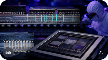
The advanced packaging taxonomy is built on 2 binding axes: 2.5D vs 3D, and interposer type. 2.5D packaging places multiple chiplets side-by-side on a silicon interposer or RDL (redistribution layer) interposer, with the interposer hosting the high-density routing between chiplets. 3D packaging stacks chiplets vertically with through-silicon-vias (TSVs) or hybrid bonding (Cu-Cu direct bonding at the wafer level), enabling the highest density and the shortest interconnect length. The 5 leading-edge architectures are: (1) TSMC CoWoS-S (silicon interposer, the original 2.5D architecture, used for H100/H200); (2) TSMC CoWoS-L (local silicon interconnect + RDL interposer, used for B100/B200/GB300); (3) TSMC CoWoS-R (RDL only, no silicon, used for cost-sensitive parts); (4) Samsung I-Cube (silicon interposer, competitive with CoWoS-S); (5) Intel EMIB (embedded multi-die interconnect bridge, the cleanest 2.5D alternative) + Foveros (3D face-to-face hybrid bonding).
The 2025-2026 advanced packaging supply-demand is structurally imbalanced. TSMC CoWoS capacity is ~38K wafers/month in 2025 and projected to ramp to ~75K wafers/month in 2026E (with the SoIC 3D packaging adding another ~10K wpm in 2026-2027E). The 2026 CoWoS capacity is ~100% allocated to the top-4 customers (Nvidia, AMD, Broadcom, Apple), and the 2027 capacity is being negotiated now. The structural supply discipline is the binding reason the advanced packaging market has held 2-3x above the historical packaging pricing curve, and the AI accelerator capex cycle is the binding demand driver. The 2026-2028 advanced packaging read-through is concentrated in the CoWoS expansion, the SoIC 3D ramp, and the substrate supply chain (Ibiden, Shinko Electric).
The packaging technology stack
Advanced packaging is built on 5 binding layers: the interposer (silicon or RDL), the chiplet integration (CoWoS / I-Cube / EMIB), the 3D hybrid bonding (Foveros / SoIC), the substrate (organic or glass), and the test/burn-in - each is a 5+ year R&D moat.
Advanced packaging technology is built on 5 binding layers. (1) The interposer: the silicon interposer (used in CoWoS-S, CoWoS-L, I-Cube) is a 100x100mm+ silicon substrate with through-silicon-vias (TSVs) and fine-pitch metal routing. The silicon interposer is manufactured on a 65nm/45nm/28nm logic process, which is the binding reason the CoWoS-S capacity is constrained by 12-inch wafer supply. The RDL interposer (used in CoWoS-R, CoWoS-L) is an organic-based routing layer with no silicon, which is cheaper but has lower routing density. The interposer technology is the binding moat for TSMC CoWoS and Samsung I-Cube. (2) The chiplet integration: the chiplets (the GPU/CPU/HBM/misc dies) are integrated onto the interposer using either flip-chip bumping (the legacy approach) or hybrid bonding (the leading-edge approach, used in 3D packaging). The chiplet integration is the binding moat for Intel Foveros and TSMC SoIC.
(3) The 3D hybrid bonding: hybrid bonding is Cu-Cu direct bonding at the wafer level, with a bonding pitch of <10 micron (vs 50-100 micron for flip-chip bumping). The 3D hybrid bonding enables the highest density and the shortest interconnect length, which is the binding reason for HBM stacking (HBM3E uses TSV-based 12-Hi stack, HBM4E uses hybrid bonding for 16-Hi). The 3D hybrid bonding is the cleanest single R&D moat for TSMC SoIC (System on Integrated Chip) and Intel Foveros. (4) The substrate: the advanced packaging substrate (the 100x100mm+ organic substrate that hosts the CoWoS/I-Cube/EMIB package) is dominated by Ibiden (~40% share), Shinko Electric (~30%), Samsung Electro-Mechanics (~15%), AT&S (~10%), and Unimicron (~5%). The substrate supply is the second binding constraint (after the interposer supply), and the substrate ASP is ~$200-500 per advanced package, vs $20-50 for a legacy package substrate.
(5) The test/burn-in: the advanced package test (including Known-Good-Die (KGD) test, final test, and burn-in) is dominated by the OSATs (Amkor, ASE Technology, JCET, Powertech Technology). The advanced package test ASP is ~$50-200 per package, which is a meaningful margin contributor for the OSATs. The 5 layers together are the binding advanced packaging technology stack, and the 5+ year R&D moat in each layer is the structural reason the 5 leading-edge suppliers control ~100% of the leading-edge market.
Advanced packaging taxonomy: 2.5D vs 3D, with interposer type
Reference points from TSMC, Samsung, Intel, and the OSATs' technology disclosures. The chart tracks the 5 leading-edge advanced packaging architectures and their binding technology.
단위: Wafers per month (12-inch equivalent)
TSMC CoWoS-S capacity 2025 (wpm)
Silicon interposer; original 2.5D; used for H100/H200
25,000
TSMC CoWoS-L capacity 2026E (wpm)
LSI + RDL interposer; used for B100/B200/GB300; 70% of 2026 mix
50,000
TSMC CoWoS-R capacity 2026E (wpm)
RDL only; cost-sensitive; ~5% of 2026 mix
5,000
TSMC SoIC 3D capacity 2026E (wpm)
3D hybrid bonding; HBM4E + 3D logic; 2026 ramp
10,000
Samsung I-Cube capacity 2026E (wpm)
Silicon interposer; competitive with CoWoS-S
8,000
Intel EMIB + Foveros 2026E (wpm)
EMIB = 2.5D bridge; Foveros = 3D hybrid bonding
8,000
OSATs (Amkor+ASE+JCET) 2026E (wpm)
Test + burn-in + advanced substrate
4,000
TSMC vs Samsung vs Intel vs the OSATs
TSMC is the cleanest advanced packaging pure-play with ~75% share, Samsung is at ~10% with I-Cube, Intel is at ~10% with EMIB + Foveros, and the OSATs (Amkor, ASE) are the test/burn-in leg - and the 2026-2028 supply is 100% allocated.
TSMC is the cleanest advanced packaging pure-play with ~75% revenue share, dominated by CoWoS. TSMC's advanced packaging capacity is concentrated at the Tainan fab (the original CoWoS site), the Hsinchu advanced packaging center (the CoWoS-L + SoIC site), and the new Arizona advanced packaging center (the US-domiciled CoWoS site, ramping 2027-2028E). TSMC's CoWoS capacity is ramping from ~38K wafers/month in 2025 to ~75K wafers/month in 2026E to ~110K wafers/month in 2027-2028E. The CoWoS-L mix is ~70% of 2026E capacity, CoWoS-S is ~25%, and CoWoS-R is ~5%. The SoIC 3D packaging (used for HBM4E stacking and 3D logic) is ramping from ~5K wafers/month in 2026E to ~25K wafers/month in 2028E. The TSMC advanced packaging capex is projected at $20-25B in 2025-2027, which is the cleanest single read on the AI capex cycle's packaging leg.
Samsung Electronics is the second-largest advanced packaging supplier with ~10% revenue share, dominated by I-Cube. Samsung's I-Cube architecture is competitive with TSMC CoWoS-S, and the I-Cube 2.0 (with local silicon interconnect, competitive with CoWoS-L) is sampling in 2026. Samsung's advanced packaging capacity is concentrated at Hwaseong (the original I-Cube site) and the new Cheonan advanced packaging center (the I-Cube 2.0 + 3D site, ramping 2027-2028E). Samsung's I-Cube capacity is ramping from ~3K wafers/month in 2025 to ~8K wafers/month in 2026E to ~15K wafers/month in 2028E. Samsung's I-Cube customers include Nvidia (some HBM3E base die), Broadcom (some custom ASICs), and the Samsung internal LSI division (Exynos + image sensors). Samsung's advanced packaging capex is projected at $3-5B in 2025-2027.
Intel is the third-largest advanced packaging supplier with ~10% revenue share, dominated by EMIB (2.5D) + Foveros (3D). Intel's EMIB architecture is the cleanest 2.5D alternative to CoWoS-S, and the Foveros architecture is the cleanest 3D hybrid bonding alternative to TSMC SoIC. Intel's advanced packaging capacity is concentrated at the Oregon D1X fab (the EMIB + Foveros site) and the new Arizona fab (the 18A + EMIB + Foveros site, ramping 2027-2028E). Intel's EMIB + Foveros customers include Intel internal (Meteor Lake + Arrow Lake + Lunar Lake + Panther Lake), Broadcom (some custom ASICs), and the Intel Foundry Services (IFS) external customers. The OSATs (Amkor, ASE Technology, JCET) are the test/burn-in + advanced substrate leg with ~5% combined share. Amkor is the cleanest US-listed advanced packaging OSAT with the new Arizona advanced packaging site (project announced 2024, ramping 2026-2027E).
| Supplier | Ticker | Share 2025 | Capacity 2026E | Capex 2025-2027 | Leading Architecture |
|---|---|---|---|---|---|
| TSMC | TSM | ~75% | ~75K wpm CoWoS + 10K wpm SoIC | $20-25B | CoWoS-S/L/R + SoIC 3D |
| Samsung Electronics | 005930.KS | ~10% | ~8K wpm I-Cube | $3-5B | I-Cube + I-Cube 2.0 |
| Intel | INTC | ~10% | ~8K wpm EMIB + Foveros | $3-5B | EMIB (2.5D) + Foveros (3D) |
| Amkor | AMKR | ~2% | Test + advanced substrate | $1-2B | OSAT + Arizona advanced pkg |
| ASE Technology | ASX | ~2% | Test + advanced substrate | $1-2B | OSAT + Taiwan advanced pkg |
| JCET | 600584.SH | ~1% | Test + advanced substrate | $0.5-1B | OSAT + China advanced pkg |
| Others | - | <1% | Test + advanced substrate | n/a | Powertech, etc. |
The substrate supply chain and customer concentration
The advanced packaging substrate is dominated by Ibiden + Shinko Electric (~70% combined), and the customer base is Nvidia (~55%) + AMD (~18%) + Broadcom (~12%) + Apple (~5%) = ~90% of demand.
The advanced packaging substrate (the 100x100mm+ organic substrate that hosts the CoWoS/I-Cube/EMIB package) is the second binding constraint after the interposer supply. The substrate supply is dominated by 5 vendors: Ibiden (~40% share, the cleanest leading-edge ABF substrate supplier), Shinko Electric (~30%, the second cleanest leading-edge supplier), Samsung Electro-Mechanics (~15%, the Samsung internal supplier), AT&S (~10%, the European substrate supplier), and Unimicron (~5%, the Taiwan substrate supplier). The advanced substrate ASP is ~$200-500 per advanced package, vs $20-50 for a legacy package substrate, and the advanced substrate supply is 100% allocated through 2026.
The customer base is structurally concentrated in 4 names: Nvidia (~55% of advanced packaging demand, for H100/H200/B100/B200/GB300 + Rubin), AMD (~18%, for MI300/MI325/MI350), Broadcom (~12%, for custom ASICs at Google, Meta, Microsoft, Amazon), and Apple (~5%, for M-series + A-series + Neural Engine). The top-4 customers are ~90% of advanced packaging demand, and the customer concentration is the structural reason the 2026-2028 advanced packaging capacity is 100% allocated.
The 2026-2028 advanced packaging demand is the cleanest single read on the AI capex cycle. The 2026 demand is ~$65-75B (up from ~$50B in 2025), the 2027 demand is ~$80-90B, and the 2028 demand is ~$90-100B. The demand growth is driven by: (1) the Nvidia Rubin ramp in 2026-2027 (each Rubin GPU needs ~1 CoWoS-L + 4-8 HBM4 + 1 base die); (2) the AMD MI400 ramp in 2027-2028 (similar CoWoS-L + HBM4 architecture); (3) the Broadcom custom ASIC ramp (each ASIC needs CoWoS-S or CoWoS-L); (4) the Apple M6/A20/Neural Engine ramp. The 2026-2028 advanced packaging demand at ~25% CAGR is the cleanest single read on the AI capex cycle's packaging leg.
Advanced packaging customer base 2026E: top-4 = 90% of demand
Reference points from the 5 advanced packaging suppliers' customer disclosures and AI accelerator shipment data. The chart tracks the structural customer concentration of advanced packaging demand.
단위: Percent of demand / USD billions
Nvidia 2026E (%)
H100/H200/B100/B200/GB300 + Rubin ramp
55
AMD 2026E (%)
MI300/MI325/MI350 + MI400 sampling
18
Broadcom 2026E (%)
Custom ASICs (Google, Meta, MSFT, AMZN)
12
Apple 2026E (%)
M-series + A-series + Neural Engine
5
Others 2026E (%)
Intel, Samsung internal, Marvell, etc.
10
Advanced pkg market 2025 ($B)
Yole; ~+25% YoY vs 2024
50
Advanced pkg market 2026E ($B)
Yole projection; +40% YoY
70
Advanced pkg market 2028E ($B)
Yole projection; +25% CAGR 2025-2028
95
Top experts, expansion, and read-throughs
Advanced packaging experts are concentrated at TSMC Tainan + Hsinchu, Samsung Hwaseong + Cheonan, and Intel Oregon D1X - and the 2026-2028 CoWoS + SoIC ramp is the cleanest single read on the AI capex stack.
The advanced packaging expert pool is structurally concentrated in 3 leading-edge IDMs + the top substrate suppliers. At TSMC, the top advanced packaging experts are: VP of R&D Dr. Y.J. Mii, Head of Advanced Packaging Dr. K.C. Hsu, Head of SoIC Dr. Shang-Yi Chiang (former), and Head of Tainan Advanced Packaging Dr. Marvin Liao. The TSMC advanced packaging team is ~3,500 engineers at Tainan + Hsinchu. At Samsung Electronics, the top advanced packaging experts are: Head of Foundry Dr. Han Seung-hoon, Head of I-Cube Dr. Kim Jae-hyun, and Head of Cheonan Packaging Dr. Park Sang-wook. The Samsung advanced packaging team is ~1,500 engineers at Hwaseong + Cheonan. At Intel, the top advanced packaging experts are: Head of Assembly/Test Dr. Babak Sabi (former), Head of EMIB Dr. Johanna Swan, and Head of Foveros Dr. Kim Hyo-jin. The Intel advanced packaging team is ~1,500 engineers at Oregon D1X + Arizona.
At the substrate suppliers, the top experts are: at Ibiden, Head of Substrate R&D Dr. Toshihiro Kishi; at Shinko Electric, Head of Substrate R&D Dr. Kenji Yamada. At the OSATs, the top experts are: at Amkor, CTO Dr. ChoonHeung Lee (former), Head of Advanced Packaging Dr. Yung-Han Chiu; at ASE Technology, CTO Dr. Tien Wu. The substrate + OSAT expert pool is ~3,000 engineers, and the geographic concentration is in Japan (Ibiden, Shinko) + Taiwan (ASE, Amkor Taiwan) + US (Amkor Arizona) + Korea (Samsung Electro-Mechanics) + China (JCET).
The 2026-2028 advanced packaging read-through is concentrated in 5 trades. (1) TSMC is the cleanest advanced packaging pure-play with ~75% share; the CoWoS-L + SoIC ramp is the cleanest single re-rating catalyst. (2) Samsung Electronics is the second advanced packaging supplier with I-Cube 2.0; the qualification at Nvidia + Broadcom is the binding test. (3) Intel is the third advanced packaging supplier with EMIB + Foveros; the IFS external customer wins are the binding test. (4) Ibiden and Shinko Electric are the cleanest advanced substrate exposures; the CoWoS-L + EMIB ramp is the binding demand driver. (5) Amkor and ASE Technology are the cleanest advanced packaging OSAT exposures; the Arizona + Taiwan advanced packaging capex is the binding growth driver. The 2026-2028 advanced packaging demand at ~25% CAGR is the cleanest single read on the AI capex cycle's packaging leg.
- Advanced packaging market: ~$50B in 2025; projected $90-100B by 2028E (~25% CAGR); 5 leading-edge suppliers (TSMC 75%, Samsung 10%, Intel 10%, OSATs 5%).
- CoWoS capacity: ~38K wpm 2025 -> ~75K wpm 2026E -> ~110K wpm 2027-2028E; CoWoS-L is ~70% of 2026 mix; SoIC 3D ramping 2026-2028E.
- Customer concentration: Nvidia ~55%, AMD ~18%, Broadcom ~12%, Apple ~5% = ~90% of demand.
- Substrate supply: Ibiden ~40% + Shinko Electric ~30% + Samsung Electro-Mechanics ~15% + AT&S ~10% + Unimicron ~5%.
- Capex 2025-2027: $30B+ combined; TSMC $20-25B, Samsung $3-5B, Intel $3-5B, Amkor $1-2B, ASE $1-2B.
- Top experts: TSMC Y.J. Mii, K.C. Hsu; Samsung Han Seung-hoon, Kim Jae-hyun; Intel Johanna Swan, Kim Hyo-jin; Ibiden Kishi; Shinko Yamada.
- Read-through: TSMC cleanest pure-play; Samsung + Intel I-Cube/EMIB challenge; Ibiden + Shinko cleanest substrate; Amkor + ASE cleanest OSAT.
What to watch
Watch the CoWoS-L capacity ramp, the SoIC 3D sampling, the Samsung I-Cube 2.0 qualification, the Intel Foveros IFS wins, the Ibiden + Shinko substrate capex, and the Rubin + MI400 customer allocation.
The first tell is the TSMC CoWoS-L capacity ramp. CoWoS-L is ~70% of the 2026 CoWoS mix, and a clean ramp from ~38K wpm 2025 to ~75K wpm 2026E to ~110K wpm 2027-2028E is a re-rating catalyst. Watch the quarterly CoWoS capacity disclosure as the cleanest single read on the AI capex cycle's packaging leg.
The second tell is the TSMC SoIC 3D sampling. SoIC 3D is the next-generation 3D hybrid bonding architecture, used for HBM4E stacking (16-Hi) and 3D logic. A clean SoIC sampling in 2026-2027 is a re-rating catalyst for TSMC; a slow SoIC ramp is a multiple-compression event. The third tell is the Samsung Electronics I-Cube 2.0 qualification. I-Cube 2.0 (with local silicon interconnect, competitive with CoWoS-L) is sampling in 2026; a clean qualification at Nvidia or Broadcom is a re-rating catalyst for Samsung, a qualification failure is a multiple-compression event. The fourth tell is the Intel Foveros IFS wins. Foveros is the cleanest 3D hybrid bonding alternative to TSMC SoIC; IFS external customer wins (e.g., Broadcom, Microsoft Maia, Amazon Trainium) are the binding test for the Intel Foundry thesis. The fifth tell is the Ibiden + Shinko Electric substrate capex. The advanced substrate is the second binding constraint after the interposer; a clean capex ramp at Ibiden + Shinko is a re-rating catalyst for the substrate cohort. The sixth tell is the Nvidia Rubin + AMD MI400 customer allocation. The Rubin + MI400 2027 CoWoS-L allocation is being negotiated now; a clean allocation across TSMC + Samsung is a re-rating catalyst, a TSMC-dominant allocation is a multiple-compression event for Samsung.