
%22%2F%3E%0A%20%20%3Ccircle%20cx%3D%22220%22%20cy%3D%22150%22%20r%3D%22180%22%20fill%3D%22%2322d3ee%22%20fill-opacity%3D%220.12%22%2F%3E%0A%20%20%3Ccircle%20cx%3D%221010%22%20cy%3D%22130%22%20r%3D%22220%22%20fill%3D%22%2338bdf8%22%20fill-opacity%3D%220.08%22%2F%3E%0A%20%20%3Ccircle%20cx%3D%22920%22%20cy%3D%22520%22%20r%3D%22170%22%20fill%3D%22%2322d3ee%22%20fill-opacity%3D%220.06%22%2F%3E%0A%20%20%3Cpath%20d%3D%22M140%20430h920%22%20stroke%3D%22url(%23line)%22%20stroke-width%3D%2212%22%20stroke-linecap%3D%22round%22%2F%3E%0A%20%20%3Cpath%20d%3D%22M220%20360c120-150%20260-220%20380-220s260%2070%20380%20220%22%20fill%3D%22none%22%20stroke%3D%22%2367e8f9%22%20stroke-opacity%3D%220.5%22%20stroke-width%3D%2216%22%20stroke-linecap%3D%22round%22%20stroke-linejoin%3D%22round%22%2F%3E%0A%20%20%3Cpath%20d%3D%22M300%20398h600%22%20stroke%3D%22%2394a3b8%22%20stroke-opacity%3D%220.24%22%20stroke-width%3D%228%22%20stroke-linecap%3D%22round%22%2F%3E%0A%20%20%3Ctext%20x%3D%22220%22%20y%3D%22510%22%20fill%3D%22%23e2e8f0%22%20fill-opacity%3D%220.7%22%20font-family%3D%22Arial%2C%20Helvetica%2C%20sans-serif%22%20font-size%3D%2238%22%20letter-spacing%3D%228%22%3EINSIGHTS%3C%2Ftext%3E%0A%3C%2Fsvg%3E)
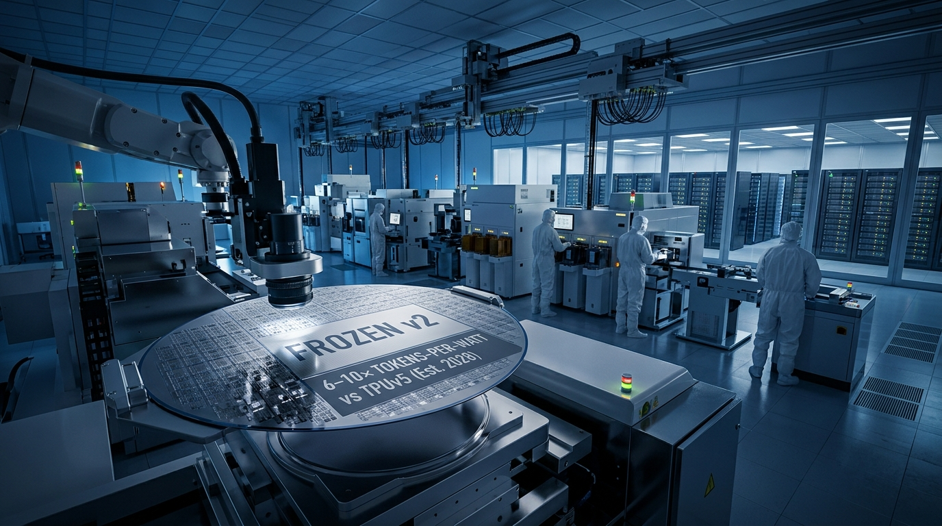
Google’s AI chip strategy just moved from “better accelerators” to “model-aware silicon.” The reported “Frozen v2” roadmap targets a step-change in inference efficiency (6–10× tokens-per-watt) and pushes deployment toward 2028, signaling that the next battle in AI infrastructure may be won by those who reduce power per token—not just compute FLOPs.
Reported project name
Frozen v2
Internal server chip (informally dubbed), reported by Reuters citing The Information
Target deployment
As early as 2028
Engineering/design still being finalized per report snippets
Efficiency goal
6–10×
AI tokens served per unit of power vs. Google’s latest custom chips
Role vs. TPUs
Complement
Designed to complement, not replace, the existing TPU line
What happened (and what’s actually new)
Google isn’t only optimizing Gemini software—it’s trying to hardwire Gemini into inference hardware
The load-bearing novelty is the “Gemini-aware hardware” idea: Reuters (citing The Information) reports “Frozen v2” aims to incorporate elements of the Gemini AI model directly into chip architecture. That’s a different optimization target than general-purpose accelerator throughput—because it can reduce energy wasted on generic execution paths.
Frozen v2: key claims to anchor your expectations
Chip
Frozen v2 (internal server chip)
Reported by Reuters citing The Information
Deployment timing
Targeted for 2028
As early as 2028 per reporting
Metric
Tokens per unit of power
Efficiency measured as AI tokens served per power
Expected improvement
6–10×
Relative to Google’s latest custom AI chips
Strategic positioning
Complement TPUs
Not a replacement; part of a broader compute-stack control push
The mechanism
How Gemini-aware silicon can realistically produce 6–10× tokens-per-watt (and where the risk hides)
A 6–10× jump in tokens-per-watt is only plausible if “Frozen v2” reduces energy in at least two places at once: (1) fewer cycles per token through model-structured execution, and (2) lower memory movement and control overhead via tighter hardware-software coupling. The risk is that gains on a subset of workloads may not generalize to the full Gemini inference mix.
- Tokens-per-watt is dominated by energy per effective token, which typically includes compute + memory + orchestration. Model-aware hardware can target the orchestration and dataflow parts, not only math throughput.
- If chip architecture incorporates “elements” of Gemini, it can reduce wasted execution on generic paths (e.g., specialized decode/update flows, structured attention handling, or hardwired routing).
- Complementing TPUs suggests a heterogeneous strategy: Frozen v2 could take the “most power-hungry” inference slices, while TPUs cover flexibility or other model families—limiting software-migration risk.
| Requirement | What the claim implies | Why it matters for investors | What to watch next |
|---|---|---|---|
| Comparable benchmark scope | Efficiency measured on representative Gemini inference workloads | Otherwise, 6–10× could be an apples-to-oranges lab result | Later disclosures: workload mix, batch sizes, sequence lengths, KV-cache handling assumptions |
| Memory-movement reduction | Lower energy spent on moving weights/activations and managing KV cache | Because memory bandwidth/latency often limits real tokens-per-watt | Signs of advanced on-package/high-bandwidth memory integration and system-level design |
| Thermal/power headroom at scale | Tokens-per-watt maintained under datacenter cooling and power delivery constraints | Datacenter power caps can erase “bench” advantages | Any system-level power envelope specs, rack-level density statements |
| Software maturity | Compilers/runtime able to exploit hardware model hooks reliably | Without tooling, hardware targets can’t be realized | Early adoption in Google services and performance regression stability |
Fundamentals + capacity context (where this matters inside Alphabet)
Alphabet has the cash generation to fund an internal compute stack—but execution still decides the ROI
Even without Frozen v2 operating metrics, the financial setup matters: Alphabet shows strong operating cash generation and substantial ongoing capex capacity. The investment question becomes whether improved inference efficiency translates into lower cost per token (and thus more margin or more capacity for demand) rather than simply shifting the constraint from chips to power delivery, networking, or utilization.
Alphabet (TTM) operating cash flow
$174.4B
Net cash provided by operating activities (TTM snapshot)
Alphabet (TTM) capex
$109.9B
Investments in property, plant & equipment (TTM)
Alphabet (TTM) free cash flow
$64.4B
Free cash flow (TTM)
Balance sheet cushion (TTM)
$380.6B
Total assets (TTM) and $126.8B cash + short-term investments
Alphabet cash capacity: operating cash flow and free cash flow (FY 2023–TTM 2026)
Use this to frame whether Alphabet can self-fund multi-year compute refresh cycles while sustaining AI capex.
Unidad: USD
Alphabet Operating cash flow (FY 2023)
Net cash provided by operating activities
101,746,000,000
Alphabet Operating cash flow (FY 2024)
Net cash provided by operating activities
125,299,000,000
Alphabet Operating cash flow (FY 2025)
Net cash provided by operating activities
164,713,000,000
Alphabet Operating cash flow (TTM 2026)
Net cash provided by operating activities
174,353,000,000
Alphabet Free cash flow (FY 2023)
Free cash flow
69,495,000,000
Alphabet Free cash flow (FY 2024)
Free cash flow
72,764,000,000
Alphabet Free cash flow (FY 2025)
Free cash flow
73,266,000,000
Alphabet Free cash flow (TTM 2026)
Free cash flow
64,429,000,000
Supply chain + who benefits/loses
This pushes demand toward advanced packaging and datacenter integration—not just leading-edge wafers
A Gemini-aware server chip is still a server platform, which means the supply chain story is bigger than “one chip design.” If Frozen v2 truly targets 6–10× better tokens-per-watt, it likely increases the importance of memory bandwidth, power delivery, and packaging integration—areas where TSMC is positioned as a critical manufacturing/packaging partner for advanced AI compute platforms.
| Layer | What changes with Frozen v2 | Why it matters for efficiency | Example public beneficiaries (tickers resolved) |
|---|---|---|---|
| Wafer fabrication | More advanced process nodes or specialized silicon options for performance-per-watt | Directly impacts transistor efficiency and high-frequency behavior | TSMC |
| Advanced packaging / system integration | Higher bandwidth memory and tighter thermal/power design in a server form factor | Real tokens-per-watt is often memory + packaging energy, not only compute | TSMC |
| Datacenter power + thermal infrastructure | Potential rack density changes and power delivery design for higher efficiency chips | If power delivery caps are reached, chips can’t express their efficiency | Not modeled here (no additional tickers in the brief) |
| Server OEM / integration | Custom boards/cooling/power rails to match Frozen v2’s power profile | System-level integration determines real tokens-per-watt in deployed racks | Not modeled here (no additional tickers in the brief) |
- Upstream: If TSMC supports Frozen v2 wafer + packaging steps, then any design shift that improves bandwidth or thermal density can increase value capture in advanced packaging volumes.
- Downstream (customers of compute): Google Cloud inference consumers may see lower cost per query if utilization and pricing enable it—otherwise the benefit may mostly accrue to Google’s internal cost structure.
- Competitive implication: the chip is designed to complement TPUs, meaning Google can tune deployment by workload class rather than forcing a single architecture across all inference.
Competitive positioning
The “Nvidia alternative” thesis depends on system-level economics, not just tokens-per-watt in a vacuum
If Frozen v2 delivers the targeted energy efficiency at scale, it can undercut competing inference stacks that rely on general-purpose accelerators. But investors should avoid the trap of assuming better chips automatically win: real economics depend on how much capacity Google can actually sell or allocate, how quickly it can migrate workloads, and whether power/cooling and networking bottlenecks dominate.
| Signal | What would confirm it | What would falsify it | Why it matters |
|---|---|---|---|
| Latency + throughput parity | Google can serve Gemini workloads with equal or better end-to-end latency under the same power cap | Efficiency gains come with unacceptable latency or throttling | Cloud buyers optimize for SLA and user experience, not only energy |
| Utilization improvements | System deployment raises effective tokens-per-watt at rack level | Compute stays underutilized due to scheduling or workload mismatch | Unutilized accelerators turn theoretical gains into idle power costs |
| Pricing/unit-economics impact | Lower cost per token feeds into either margin expansion or more capacity for demand | Savings are absorbed internally without monetization or capacity release | Determines shareholder impact, not just engineering success |
| Heterogeneous deployment effectiveness | Frozen v2 complements TPU usage with a clear workload partition | Architecture overlap creates internal complexity and lowers overall efficiency | Complementing TPUs only helps if the division of labor is coherent |
Investable view (1–3 year horizon)
Google’s next equity catalyst is whether tokens-per-watt becomes a repeatable, monetizable cost advantage
Frozen v2 is a forward-looking project (2028 target), so the near-term catalyst is less about immediate financial numbers and more about direction of travel: AI compute bottlenecks, datacenter capex efficiency, and any early internal deployment learnings that reduce uncertainty about realization.
- Base case (data-driven): If Google sustains strong cash generation (operating cash flow) while funding capex, it can absorb schedule and performance risks long enough to reach 2028.
- Upside case: Model-aware silicon reduces cost per token meaningfully and measurably; then internal compute economics can support either lower prices or higher capacity for demand growth.
- Downside case: Bench efficiency fails to translate to system-level tokens-per-watt due to memory/network/thermal constraints or workload mismatch—making the chip a niche improvement rather than an inflection.