
%22%2F%3E%0A%20%20%3Ccircle%20cx%3D%22220%22%20cy%3D%22150%22%20r%3D%22180%22%20fill%3D%22%2322d3ee%22%20fill-opacity%3D%220.12%22%2F%3E%0A%20%20%3Ccircle%20cx%3D%221010%22%20cy%3D%22130%22%20r%3D%22220%22%20fill%3D%22%2338bdf8%22%20fill-opacity%3D%220.08%22%2F%3E%0A%20%20%3Ccircle%20cx%3D%22920%22%20cy%3D%22520%22%20r%3D%22170%22%20fill%3D%22%2322d3ee%22%20fill-opacity%3D%220.06%22%2F%3E%0A%20%20%3Cpath%20d%3D%22M140%20430h920%22%20stroke%3D%22url(%23line)%22%20stroke-width%3D%2212%22%20stroke-linecap%3D%22round%22%2F%3E%0A%20%20%3Cpath%20d%3D%22M220%20360c120-150%20260-220%20380-220s260%2070%20380%20220%22%20fill%3D%22none%22%20stroke%3D%22%2367e8f9%22%20stroke-opacity%3D%220.5%22%20stroke-width%3D%2216%22%20stroke-linecap%3D%22round%22%20stroke-linejoin%3D%22round%22%2F%3E%0A%20%20%3Cpath%20d%3D%22M300%20398h600%22%20stroke%3D%22%2394a3b8%22%20stroke-opacity%3D%220.24%22%20stroke-width%3D%228%22%20stroke-linecap%3D%22round%22%2F%3E%0A%20%20%3Ctext%20x%3D%22220%22%20y%3D%22510%22%20fill%3D%22%23e2e8f0%22%20fill-opacity%3D%220.7%22%20font-family%3D%22Arial%2C%20Helvetica%2C%20sans-serif%22%20font-size%3D%2238%22%20letter-spacing%3D%228%22%3EINSIGHTS%3C%2Ftext%3E%0A%3C%2Fsvg%3E)
Industry structure
EUV is a 100% monopoly industry - ASML is the only merchant supplier, the customer base is 4 IDMs (TSMC, Samsung, Intel, SK hynix), and the 2026-2028 supply is 100% allocated.
EUV (Extreme Ultraviolet) lithography is the binding constraint of the entire leading-edge semiconductor industry, and the supply chain is a literal monopoly. ASML (Veldhoven, Netherlands) is the only merchant EUV supplier in the world, with ~5,000 EUV engineers at its Veldhoven campus, ~$30B in 2025 EUV system + service revenue, and 100% merchant EUV market share. The EUV customer base is structurally concentrated in 4 IDMs: TSMC (~55% of EUV system revenue), Samsung Electronics (~20%), Intel (~15%), and SK hynix (~10%). No other company in the world can manufacture an EUV scanner, and the technology moat is built on 30+ years of R&D, $10B+ in cumulative capex, and a network of ~5,000 suppliers (the most critical being Carl Zeiss SMT for the projection optics).
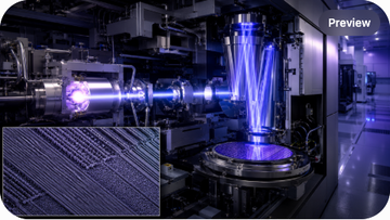
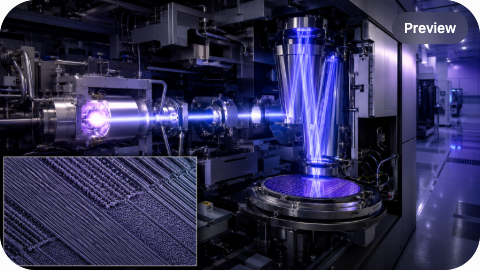
The EUV system is the most complex machine humans have ever built. A TWINSCAN NXE:3800E EUV system has ~100,000 parts, ~3,000 cables, and weighs ~150 tons. The system uses a tin droplet laser-produced plasma (LPP) light source that fires 50,000 times per second to generate 13.5nm EUV light, which is collected by a Zeiss multilayer mirror (the most precise mirror ever manufactured, with 0.5 nm surface accuracy), and projected onto a wafer through a 4x-6x reduction optics. The wafer stage moves at 0.5g acceleration and 1 m/s velocity, with overlay accuracy of <1 nm. The reticle (mask) stage is held in a vacuum chamber with the EUV light; the pellicle (a thin membrane that protects the reticle from particles) is the most fragile component in the system.
The 2025-2026 EUV demand is 100% sold out. ASML guided Q1 2026 to ~50 EUV system shipments (revenue ~$10B in the quarter), with 2026 full-year EUV revenue projected at $32-35B. The 2027-2028 demand is even stronger, with High-NA EUV (TWINSCAN EXE:5000) ramping in 2026-2028. The High-NA EUV system is priced at ~$380M each (vs $200M for standard EUV), and the first 4 systems were delivered to Intel (Oregon D1X), TSMC (Hsinchu R1), Samsung (Hwaseong), and SK hynix (M16) in 2024-2025. The 2026-2028 High-NA demand is the cleanest single read on the 2nm/1.4nm/1nm logic roadmap.
The EUV technology stack
EUV is built on 5 binding layers: the tin droplet LPP source, the Zeiss multilayer mirror, the reticle, the photoresist, and the wafer stage - each of which is a 10+ year R&D moat.
The EUV technology stack has 5 binding layers. (1) The light source: ASML's EUV source uses a tin droplet (25 micron diameter) fired at 70 m/s through a vacuum chamber; a high-power CO2 laser (40+ kW peak, multi-kW average) hits the droplet to create a tin plasma that emits 13.5nm EUV light. The source power has scaled from 250W (NXE:3400) to 500W+ (NXE:3800E), with High-NA EXE:5000 targeting 1,000W+ in 2027-2028. The tin plasma is the binding physics constraint; the conversion efficiency from laser power to EUV light is ~3-5%, which is why the source needs 40+ kW of laser power to generate 500W of EUV light. (2) The collector mirror: the Carl Zeiss SMT collector is a multilayer (Mo/Si, 50+ bilayers) grazing-incidence mirror that collects the EUV light from the plasma. The collector is the most precise mirror ever manufactured, with 0.5 nm surface accuracy and 70%+ reflectivity at 13.5nm. Zeiss has spent 20+ years and $5B+ in cumulative R&D on EUV optics.
(3) The reticle (mask): the EUV reticle is a 6-inch square quartz substrate with a patterned absorber (typically TaN or TaBN). The reticle is held in a vacuum chamber and scanned by the EUV light. The reticle is the most expensive single component in the EUV ecosystem, costing $200-400K per advanced EUV mask set, and the mask blank (the substrate) is supplied by a duopoly (Hoya and AGC). The pellicle (a thin polysilicon membrane that protects the reticle from particles) is the most fragile component; ASML's EUV pellicle was a 10+ year R&D project that finally reached production in 2023-2024. (4) The photoresist: the EUV resist is a chemically amplified resist (CAR) that is 10-30 nm thick and is exposed by the EUV light. The resist is supplied by a tight oligopoly of JSR, Shin-Etsu Chemical, Tokyo Ohka Kogyo, Sumitomo Chemical, Fujifilm, and a few Korean challengers (Dongjin Semichem). The EUV resist is the subject of a separate deep-dive.
(5) The wafer stage: the ASML wafer stage is a 6-axis air-bearing stage that moves the wafer at 0.5g acceleration and 1 m/s velocity, with overlay accuracy of <1 nm and focus accuracy of <10 nm. The stage is held in a vacuum chamber and is the cleanest single mechanical assembly in any industrial system. The wafer stage is supplied by ASML in-house (with some components from KMW and NTK). The 5 layers together are the binding EUV technology stack, and the 10+ year R&D moat in each layer is the structural reason ASML is the only merchant EUV supplier.
EUV source power scaling: from 250W to 1,000W+
Reference points from ASML technology disclosures and TechInsights teardowns. The chart tracks the EUV source power scaling that has enabled the leading-edge AI chip roadmap.
Unidad: Watts (EUV source power)
NXE:3400 (2018)
First production EUV; 250W source; 13.5nm wavelength
250
NXE:3600D (2020)
Source upgrade; 280W; 7nm/5nm logic production
280
NXE:3800E (2023)
Current leading edge; 500W; 3nm/2nm logic
500
EXE:5000 High-NA (2026-2027)
High-NA; 1,000W target; 2nm/1.4nm logic
1,000
EXE:5200 High-NA (2028-2030)
Next-gen High-NA; 1,500W target; 1nm and beyond
1,500
EUV customers and the AI capex cycle
TSMC is the cleanest EUV exposure with ~55% of system revenue, Samsung is the second at ~20%, and the 2026-2028 EUV capex is the cleanest single read on the AI capex cycle.
TSMC is the cleanest EUV exposure with ~55% of ASML EUV system revenue. TSMC operates the largest EUV installed base in the world, with ~120 EUV systems in operation at Hsinchu, Tainan, and the new Arizona fab as of Q1 2026. TSMC's EUV demand is driven by the AI accelerator capex cycle (Nvidia, AMD, Apple, Broadcom, MediaTek) and the leading-edge smartphone SoC cycle (Apple, MediaTek, Qualcomm). TSMC's 2026-2028 EUV capex is projected at $8-10B/year, with the Arizona fab ramp and the 2nm/1.4nm node ramp as the binding drivers. TSMC's first High-NA EUV system was delivered to the Hsinchu R1 in 2024 and is being used for 1.4nm/1nm R&D.
Samsung Electronics is the second-largest EUV customer at ~20% of ASML system revenue. Samsung operates ~50 EUV systems at Hwaseong, Pyeongtaek, and the new Taylor fab. Samsung's EUV demand is driven by the memory roadmap (HBM4, V-NAND V10) and the foundry roadmap (3nm/2nm Gate-All-Around). Samsung's 2026-2028 EUV capex is projected at $3-5B/year. The first High-NA EUV system was delivered to Hwaseong in 2024 and is being used for 2nm/1.4nm foundry R&D and HBM4 base-die R&D.
Intel is the third-largest EUV customer at ~15% of ASML system revenue. Intel operates ~30 EUV systems at Oregon D1X, Ireland Fab 24, and the new Arizona fab. Intel's EUV demand is driven by the Intel 18A (1.8nm) and Intel 14A (1.4nm) foundry roadmap. Intel was the first customer to receive a High-NA EUV system (Oregon D1X in 2024) and is using High-NA for 18A and 14A production. SK hynix is the fourth-largest EUV customer at ~10% of ASML system revenue. SK hynix operates ~15 EUV systems at M16 (Pyeongtaek) and M15X (Cheongju) for HBM4, HBM4E, and the V10/V11 V-NAND roadmap. SK hynix's first High-NA EUV system was delivered to M16 in 2025 for HBM4E and 1c DRAM R&D.
| Customer | Ticker | Share of EUV Rev | Installed Base | 2026-2028 Capex | High-NA EUV |
|---|---|---|---|---|---|
| TSMC | TSM | ~55% | ~120 systems | $8-10B/yr | Hsinchu R1 (1.4nm/1nm R&D) |
| Samsung Electronics | 005930.KS | ~20% | ~50 systems | $3-5B/yr | Hwaseong (2nm/1.4nm + HBM4) |
| Intel | INTC | ~15% | ~30 systems | $2-4B/yr | Oregon D1X (18A + 14A) |
| SK hynix | 000660.KS | ~10% | ~15 systems | $1-2B/yr | M16 Pyeongtaek (HBM4E + 1c DRAM) |
| Others (research) | - | <1% | ~5 systems | n/a | imec, Albany, IBM Research |
High-NA EUV and the 2026-2028 race
High-NA EUV is the 2026-2028 binding test - ASML EXE:5000 is $380M per system, the first 4 systems are at Intel, TSMC, Samsung, and SK hynix, and the 2027-2028 High-NA capacity is 100% allocated.
High-NA EUV is the next binding step in lithography. The standard EUV numerical aperture (NA) is 0.33; the High-NA EUV NA is 0.55, which provides a 2x resolution improvement (down to ~8 nm half-pitch) and enables single-exposure patterning for the 2nm/1.4nm/1nm logic nodes. The High-NA EUV system (ASML TWINSCAN EXE:5000) is priced at ~$380M per system, which is roughly 1.9x the standard EUV system. The first High-NA EUV system was delivered to Intel Oregon D1X in Q4 2024, followed by TSMC Hsinchu R1 in Q1 2025, Samsung Electronics Hwaseong in Q2 2025, and SK hynix M16 in Q3 2025. The first 4 High-NA systems are being used for 2nm/1.4nm logic R&D and HBM4E/1c DRAM R&D.
The 2026-2028 High-NA EUV ramp is the cleanest single read on the 2nm/1.4nm logic node. ASML is targeting 5-10 High-NA shipments per year in 2026-2027 and 15-20 per year in 2028-2030, with the cumulative High-NA installed base projected at ~50 systems by 2030. The 2027-2028 High-NA capacity is 100% allocated to the 4 IDMs (Intel, TSMC, Samsung, SK hynix), and the 2028-2030 allocation is being negotiated now. The High-NA EUV ramp is the binding reason the leading-edge logic node cadence has accelerated from 2.5 years/node (2015-2020) to 2 years/node (2020-2025) to 1.5-2 years/node (2025-2030).
The High-NA EUV read-through is concentrated in 5 trades. (1) ASML is the cleanest pure-play with 100% merchant EUV market share; the High-NA ramp is a structural re-rating catalyst. (2) TSMC is the largest EUV customer with the cleanest AI capex exposure; the High-NA ramp is the cleanest single read on the 2nm/1.4nm logic node. (3) Samsung Electronics is the second EUV customer with the cleanest memory EUV exposure (HBM4, V-NAND V10). (4) Intel is the cleanest US logic exposure with the first High-NA system; the 18A + 14A roadmap is the binding test. (5) SK hynix is the cleanest memory EUV exposure (HBM4E + 1c DRAM). The 2026-2028 High-NA EUV demand is the cleanest single read on the leading-edge AI capex cycle.
- EUV is a 100% monopoly: ASML is the only merchant supplier; 4 IDMs (TSMC 55%, Samsung 20%, Intel 15%, SK hynix 10%) are the customers.
- EUV system: $200M+ each; ~100,000 parts; 13.5nm wavelength; 0.33 NA; 500W+ source power; <1 nm overlay accuracy.
- High-NA EUV (EXE:5000): $380M each; 0.55 NA; 1,000W+ source; first 4 systems delivered to Intel, TSMC, Samsung, SK hynix in 2024-2025.
- 2026-2028 EUV capex: ~$15-20B/year industry; ASML 2026 EUV revenue $32-35B; High-NA adds $1.5-2B/year incremental.
- Top experts: ASML Veldhoven has ~5,000 EUV engineers; ~30% PhD-level; Martin van den Brink (CTO emeritus), Christophe Fouquet (President), Teun van Gogh (EUV source).
- EUV supply chain: ASML system integrator; Zeiss projection optics; Hoya/AGC mask blanks; JSR/Shin-Etsu/TOK/Sumitomo/Fujifilm photoresist; ~5,000 other suppliers.
- Read-through: ASML cleanest pure-play; TSMC cleanest AI capex exposure; Intel cleanest US logic; Samsung cleanest memory EUV; SK hynix cleanest HBM EUV.
What to watch
Watch the High-NA EUV shipment cadence, the 2nm/1.4nm node yield ramp, the pellicle yield curve, the source power scaling, and the next-gen Hyper-NA EUV research signals.
The first tell is the High-NA EUV shipment cadence. ASML is targeting 5-10 High-NA shipments in 2026 and 15-20 in 2028-2030. A clean 10+ shipment cadence in 2026 is a re-rating catalyst; a 5 or fewer shipment cadence is a multiple-compression event. Watch the quarterly ASML shipment data as the cleanest read on the 2nm/1.4nm logic node ramp.
The second tell is the 2nm/1.4nm node yield ramp. The first High-NA EUV systems are being used for 2nm/1.4nm R&D at Intel, TSMC, Samsung Electronics, and SK hynix. A clean yield ramp at 70%+ by 2027 is a re-rating catalyst for the AI capex stack; a yield stall at 50-60% is a multiple-compression event. The third tell is the pellicle yield curve. The EUV pellicle is the most fragile component in the system; a clean yield ramp at 80%+ is the binding test for the High-NA production ramp. The fourth tell is the source power scaling. The 500W -> 1,000W -> 1,500W roadmap is the cleanest single read on the EUV throughput; a clean 1,000W in 2026-2027 is a re-rating catalyst, a 800W stall is a multiple-compression event. The fifth tell is the Hyper-NA EUV research signals. The next-generation EUV NA target is 0.7-0.75 (Hyper-NA), which would enable single-exposure patterning for sub-1nm nodes; research signals from ASML and Carl Zeiss SMT on Hyper-NA are the cleanest single read on the post-2030 logic roadmap.