
%22%2F%3E%0A%20%20%3Ccircle%20cx%3D%22220%22%20cy%3D%22150%22%20r%3D%22180%22%20fill%3D%22%2322d3ee%22%20fill-opacity%3D%220.12%22%2F%3E%0A%20%20%3Ccircle%20cx%3D%221010%22%20cy%3D%22130%22%20r%3D%22220%22%20fill%3D%22%2338bdf8%22%20fill-opacity%3D%220.08%22%2F%3E%0A%20%20%3Ccircle%20cx%3D%22920%22%20cy%3D%22520%22%20r%3D%22170%22%20fill%3D%22%2322d3ee%22%20fill-opacity%3D%220.06%22%2F%3E%0A%20%20%3Cpath%20d%3D%22M140%20430h920%22%20stroke%3D%22url(%23line)%22%20stroke-width%3D%2212%22%20stroke-linecap%3D%22round%22%2F%3E%0A%20%20%3Cpath%20d%3D%22M220%20360c120-150%20260-220%20380-220s260%2070%20380%20220%22%20fill%3D%22none%22%20stroke%3D%22%2367e8f9%22%20stroke-opacity%3D%220.5%22%20stroke-width%3D%2216%22%20stroke-linecap%3D%22round%22%20stroke-linejoin%3D%22round%22%2F%3E%0A%20%20%3Cpath%20d%3D%22M300%20398h600%22%20stroke%3D%22%2394a3b8%22%20stroke-opacity%3D%220.24%22%20stroke-width%3D%228%22%20stroke-linecap%3D%22round%22%2F%3E%0A%20%20%3Ctext%20x%3D%22220%22%20y%3D%22510%22%20fill%3D%22%23e2e8f0%22%20fill-opacity%3D%220.7%22%20font-family%3D%22Arial%2C%20Helvetica%2C%20sans-serif%22%20font-size%3D%2238%22%20letter-spacing%3D%228%22%3EINSIGHTS%3C%2Ftext%3E%0A%3C%2Fsvg%3E)
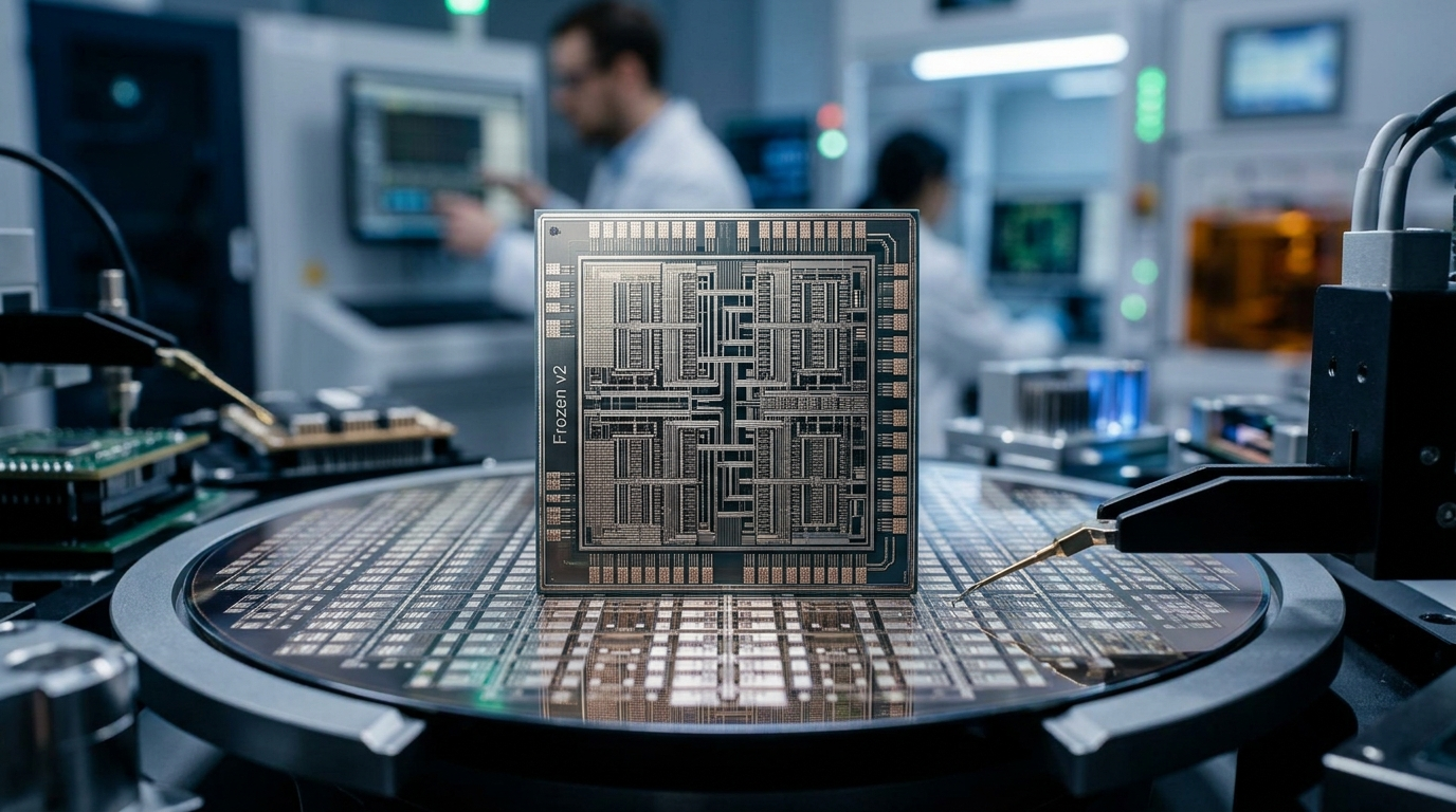
Google’s reported “Frozen v2” chip is a signal that hyperscalers are moving from “accelerate the model” to “bake the model into the silicon.” If the rumored 6–10x token-per-watt jump holds and the 2028 timing is right, the inference cost curve (and therefore capex + power demand planning) shifts again—this time targeting Gemini specifically rather than general-purpose AI compute.
Event
Frozen v2
Server chip project informally dubbed “Frozen v2” integrating Gemini elements into hardware (Reuters, 2026-07-20)
Efficiency target
6–10x
More tokens served per unit of power vs. Google’s latest custom AI chips (Reuters, 2026-07-20)
Deployment window
2028
Google expects to deploy as soon as 2028 (Reuters, 2026-07-20)
What happened
Frozen v2 reframes Google’s roadmap from “TPU upgrades” to “Gemini co-designed with hardware”
Reuters reports that Google is developing a new server chip codenamed “Frozen v2,” designed to incorporate elements of its Gemini model directly into the hardware. The key headline isn’t just a better accelerator—it’s model-specific silicon specialization aimed at inference efficiency.
Load-bearing Reuters details (the claims the market will trade on)
Codename / concept
Frozen v2
A new server chip integrating Gemini elements into silicon
Metric
Tokens per watt
Efficiency measured as tokens served per unit of power
Expected gain
6–10x
Against Google’s latest custom AI chips
Timing
As early as 2028
Targeted deployment window
Relationship to TPU
Separate track
Reuters characterizes it as a new set of homegrown chips rather than replacing the TPU roadmap
Baseline & comparison
TPU 8t/8i raises the bar—but Frozen v2 is about a different lever: tokens per watt via deeper model embedding
Google’s own Next ’26 messaging distinguishes TPU 8t (training) and TPU 8i (reasoning/inference). TPU 8i is already positioned as an inference-specialized system (including MoE-oriented design choices), but Frozen v2—if it exists as reported—targets further efficiency by pushing Gemini-specific structure into hardware.
| System | Stated purpose | Publicly cited inference-related details |
|---|---|---|
| TPU 8i | Inference and reinforcement learning / reasoning | 384 MB on-chip SRAM; 288 GB HBM3; 19.2 Tb/s ICI bandwidth; CAE reduces on-chip latency by up to 5x; “up to 80% better performance per dollar” vs prior generation; “soon” availability to Cloud customers |
| TPU 8t | Training powerhouse | Nearly 3x higher compute performance vs previous generations; 9,600 chips per superpod; 121 exaflops compute per superpod; 2 petabytes shared memory |
- Google is already productizing inference specialization with TPU 8i (performance-per-dollar improvements and low-latency engines are explicitly marketed).
- Frozen v2, per Reuters, is a further step: the efficiency lever shifts from system-level optimization to potentially architecture-level model embedding (Gemini elements baked into silicon).
- If token-per-watt truly jumps 6–10x, the economics can swing even if TPU 8i is “only” meaningfully better than Ironwood; improvements compound over rising inference demand.
Causal chain
The 6–10x claim likely implies Frozen v2 tackles inference bottlenecks beyond raw compute
A jump like 6–10x in tokens per watt usually can’t come from “more FLOPS” alone. It implies a co-design strategy that reduces wasted compute, cuts data movement, and matches silicon execution units to the dominant shapes in Gemini inference.
Where a “tokens per watt” uplift can come from (hypothesis map tied to what Google is already signaling with TPU 8i)
Not a measurement—this frames which efficiency levers are consistent with Google’s public TPU 8i design emphasis and Reuters’ Frozen v2 premise.
Unidad: relative importance (heuristic)
Lower on-chip latency / fewer cycles per token
Consistent with TPU 8i marketing for latency reduction via CAE
60
Reduced memory traffic per token (HBM/SRAM strategy)
Consistent with TPU 8i SRAM + bandwidth emphasis
50
Better fit for MoE/routing patterns
TPU 8i marketed for agentic workflows and MoE models; co-design could specialize routing
45
Hardwiring Gemini architecture elements
Directly aligned with Reuters: embed elements of Gemini into hardware
40
Impact
Frozen v2 pressures the GPU-centric stack most through inference TCO planning, not training headline benchmarks
Even if GPUs remain strong for broad training and fast iteration, an inference-specific, token-per-watt breakthrough hits the part of the P&L that matters day-to-day: serving cost at scale. That tends to shift buying from “general accelerators” toward bespoke inference silicon and the systems that wrap it.
| Layer | Likely effect of Frozen v2 (if targets are real) | Who wins / who loses (listed comparables) |
|---|---|---|
| Direct (Google/Alphabet) | Lower inference cost per token; potential to expand Gemini usage without proportional power/capacity increases | Alphabet benefits; margin and cash flow sensitivity via capex + opex efficiency |
| Downstream channel | Cloud inference pricing pressure + improved unit economics for agentic workflows | Cloud customers get lower effective cost; competition for merchant-GPU-priced inference intensifies for alternatives to Google’s stack |
| Upstream: custom silicon co-design & packaging | More reliance on ASIC/XPU co-design ecosystems and advanced packaging supply chains | Broadcom (custom AI chip co-design / infrastructure stack) likely benefits; others depend on whether they supply packaging/interconnect components |
| Upstream: mobile/edge silicon demand spillovers | Model-embedded design can create trickle-down expectations for inference efficiency across device classes | Uncertain for MediaTek without direct verification of partnership scope in this specific event; treat as a scenario, not a fact |
| Competitive compute stack (GPU-centric) | If token-per-watt rises 6–10x, GPUs face tougher economics in the “inference at hyperscaler scale” segment | NVIDIA at risk on inference share—though training and software moat may cushion |
Supply-chain view
The most important supply-chain variable is advanced co-design + packaging, not just the compute die
Google’s reported direction (model embedded in hardware) increases the probability that the differentiator sits across the stack: interconnect topology, high-bandwidth memory strategy, and high-yield packaging capable of shipping at hyperscaler volumes.
- Advanced packaging and packaging-enabled memory bandwidth are already central in Google’s TPU story (TPU 8i publicly emphasizes large HBM capacity and very high ICI bandwidth).
- If Frozen v2 is “separate from TPU” rather than “a smaller TPU upgrade,” it likely expands the set of platform-level constraints (new board/topology, new memory/per-token cycle budget), increasing spend with custom-XPU ecosystems.
- This environment tends to be favorable to companies that sit in the middle of custom accelerator co-design and the infrastructure needed to integrate dies into systems; Broadcom is the most direct listed beneficiary among your topic set.
Fundamental lens (listed companies)
Alphabet is positioned to self-fund model-silicon bets; Broadcom is levered to custom-XPU ramps; NVIDIA’s exposure depends on inference-share durability
Use the financials to map capacity to invest and where the market may re-rate exposure. Frozen v2 is a tech story, but hyperscaler silicon moves are capital- and supply-chain-intensive—so balance-sheet and operating cash flow matter.
| Company | FY revenue | FY operating cash flow | FY free cash flow | What matters for Frozen v2 read-through |
|---|---|---|---|---|
| Alphabet | $402.963B (FY2025) | $164.713B (FY2025) | $73.266B (FY2025) | Can absorb multi-year infrastructure R&D and capex; Frozen v2 aims at inference economics that scale with Gemini usage |
| Broadcom | $63.887B (FY2025) | $27.537B (FY2025) | $26.914B (FY2025) | Custom silicon ecosystem leverage; if hyperscalers increase custom inference ASIC share, Broadcom’s co-design + infrastructure positioning is structurally advantaged |
| NVIDIA | $130.497B (FY2025) | $64.089B (FY2025) | $60.853B (FY2025) | More exposed to merchant GPU inference economics; however, NVIDIA’s training breadth and software moat can cushion—effects hinge on whether inference share shifts away |
Alphabet vs Broadcom vs NVIDIA: operating cash flow as a funding indicator for long-cycle hardware bets
FY operating cash flow from the data tools used in this session.
Unidad: USD
Valuation/pricing risk to the GPU stack
If Frozen v2 delivers, GPUs face a reset in “inference per watt” competitive comparisons—especially for MoE-style workloads
The market tends to price inference silicon on throughput-per-watt and throughputs-per-dollar. Google already market-tested this with TPU 8i (up to 80% better performance per dollar than Ironwood). Frozen v2’s reported 6–10x token-per-watt target implies a potential step-change in the next round of competitive comparisons.
| Mechanism | Why it changes TCO | Most likely arena impacted |
|---|---|---|
| Higher tokens per watt | Lower power cost per token; reduces required facility capacity for a given demand | High-volume inference (Gemini serving, agentic workflows, MoE routing) |
| Lower cycles/token via model embedding | Fewer compute cycles per generated token; lowers both power and accelerator-hours demand | Latency-sensitive and high-throughput token generation |
| System-level specialization (as with TPU 8i) | Improves memory bandwidth and reduces on-chip latency; raises effective utilization | Clusters optimized for the model’s inference shape |
What to watch next (1–3 years)
The biggest milestone isn’t Frozen v2’s name—it’s any public signal that model-embedded chips are shipping into production systems
- Google Cloud availability timing: any “soon”/GA-like language for Frozen v2-class inference beyond internal pilots (Reuters says 2028 target).
- Comparative inference metrics: whether Google publishes token-per-watt, latency, or cost-per-token for Gemini-serving scenarios against existing TPU generations.
- Supply-chain triangulation: any additional reporting or supplier mentions around packaging/interconnect and custom co-design partners as Frozen v2 transitions from prototype to ramp.
- GPU allocation signals: hyperscaler capex mix commentary (e.g., whether NVIDIA orders are affected at the inference rack/system level).
Synthesis / stance
Frozen v2 is a “model-silicon co-design accelerant”—bullish for custom-ASIC ecosystems, bearish for merchant inference dominance
My base-case interpretation is that Reuters’ 6–10x token-per-watt target, if realized, pushes the industry further toward hardware that is specialized to the model family and its inference shapes. That tends to increase the value of custom co-design and advanced system integration, while forcing GPU-centric inference economics to defend their position at scale.
| Company | Primary “if true” driver | Key variable to verify |
|---|---|---|
| Alphabet | Frozen v2 reduces Gemini serving cost enough to expand usage and protect margins despite rising demand | Whether the token-per-watt uplift shows up in measurable production economics by/after 2028 |
| Broadcom | Hyperscalers increase custom inference ASIC share and keep expanding co-design/integration needs | Any event-specific supplier role expansion (not yet proven here) tied to Google/others’ model-embedded chips |
| NVIDIA | GPU inference share declines at the margin, but training breadth and software ecosystem slow the impact | Whether NVIDIA’s customer mix shifts away from inference-dominant deployments as token-per-watt becomes the dominant buyer metric |