
%22%2F%3E%0A%20%20%3Ccircle%20cx%3D%22220%22%20cy%3D%22150%22%20r%3D%22180%22%20fill%3D%22%2322d3ee%22%20fill-opacity%3D%220.12%22%2F%3E%0A%20%20%3Ccircle%20cx%3D%221010%22%20cy%3D%22130%22%20r%3D%22220%22%20fill%3D%22%2338bdf8%22%20fill-opacity%3D%220.08%22%2F%3E%0A%20%20%3Ccircle%20cx%3D%22920%22%20cy%3D%22520%22%20r%3D%22170%22%20fill%3D%22%2322d3ee%22%20fill-opacity%3D%220.06%22%2F%3E%0A%20%20%3Cpath%20d%3D%22M140%20430h920%22%20stroke%3D%22url(%23line)%22%20stroke-width%3D%2212%22%20stroke-linecap%3D%22round%22%2F%3E%0A%20%20%3Cpath%20d%3D%22M220%20360c120-150%20260-220%20380-220s260%2070%20380%20220%22%20fill%3D%22none%22%20stroke%3D%22%2367e8f9%22%20stroke-opacity%3D%220.5%22%20stroke-width%3D%2216%22%20stroke-linecap%3D%22round%22%20stroke-linejoin%3D%22round%22%2F%3E%0A%20%20%3Cpath%20d%3D%22M300%20398h600%22%20stroke%3D%22%2394a3b8%22%20stroke-opacity%3D%220.24%22%20stroke-width%3D%228%22%20stroke-linecap%3D%22round%22%2F%3E%0A%20%20%3Ctext%20x%3D%22220%22%20y%3D%22510%22%20fill%3D%22%23e2e8f0%22%20fill-opacity%3D%220.7%22%20font-family%3D%22Arial%2C%20Helvetica%2C%20sans-serif%22%20font-size%3D%2238%22%20letter-spacing%3D%228%22%3EINSIGHTS%3C%2Ftext%3E%0A%3C%2Fsvg%3E)
Bottom line
EUV is a system of bottlenecks, not a single machine.
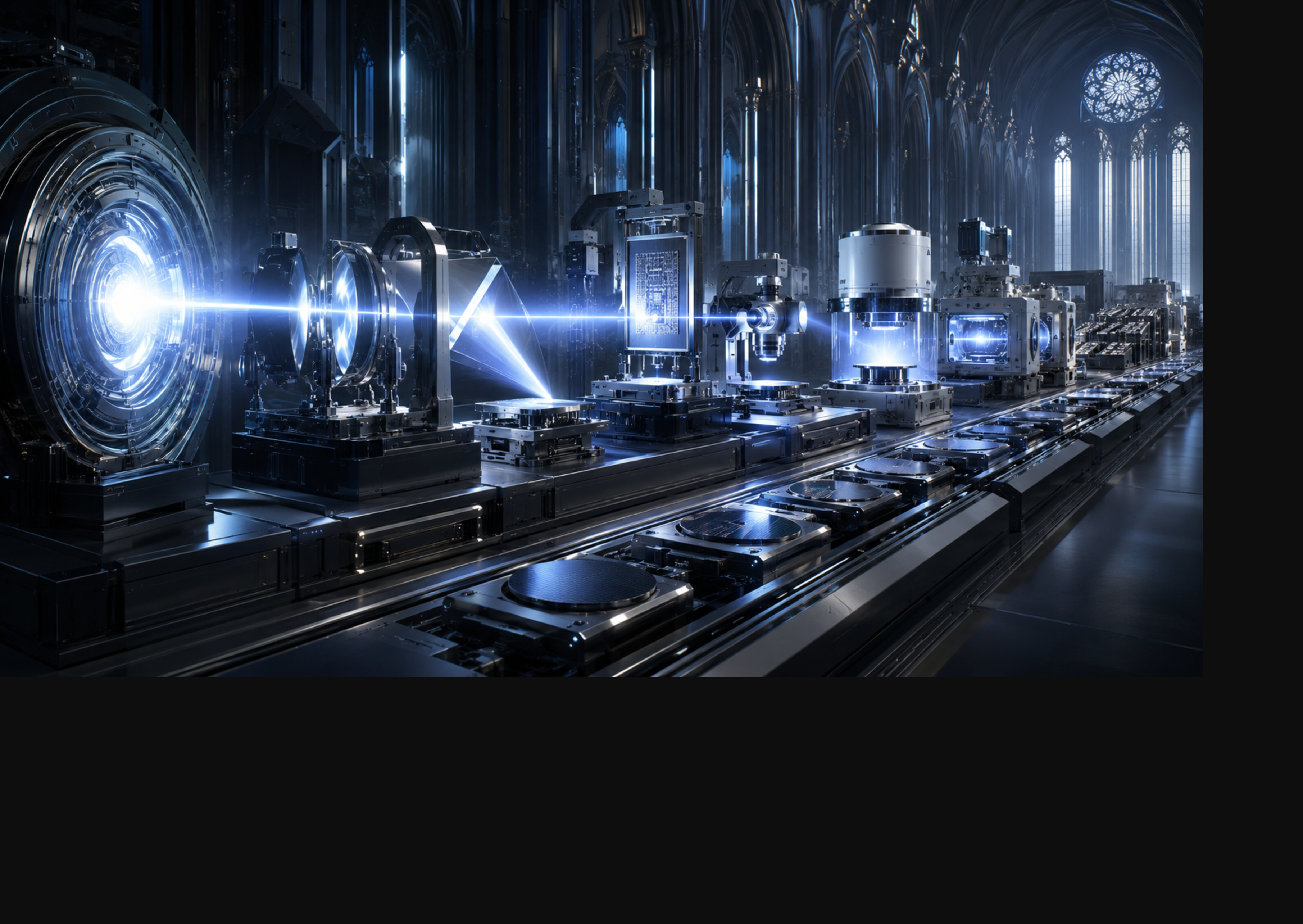
It is tempting to talk about EUV as if it were a single box on a factory floor. It is not. ASML, ZEISS, resist vendors, metrology specialists, and fab operators each control a different link in the chain that turns light into advanced logic and memory wafers.
That matters because the value is distributed unevenly. A scanner can be brilliant and still not solve the whole problem if masks, resist, inspection, or downstream capacity lag behind.
Shipment mix
ASML's 2025 shipment mix shows the headline is only the start of the story.
The company shipped 48 EUV systems, 279 DUV systems, and 208 metrology or inspection systems in 2025. That spread is important because the market often focuses only on EUV, even though the rest of the stack is what makes EUV yield and capacity expansion real.
The first full-spec High-NA system is another signal. High-NA is not a generic upgrade. It is a next-step capability that raises the bar for every supplier around the scanner.
ASML ships a wider tool stack than the EUV headline suggests
2025 shipment mix. The point is not the absolute scale of each category; it is how much supporting equipment is required around the leading-edge scanner base.
단위: systems
Chokepoints
Every stage of the lithography flow has a different owner and a different constraint.
ZEISS owns the mirror and optics challenge. TOK and other materials suppliers own the resist and process chemistry challenge. Metrology and inspection vendors own the defect-detection challenge. Mask shops and fab operators own the pattern-fidelity and throughput challenge.
The result is a chain where one weak link can slow the entire line. That is why EUV pricing is sticky and why new capacity takes so long to convert into actual wafer output.
| Link in the chain | Constraint | Why it matters |
|---|---|---|
| Light source | Stability and uptime | Throughput collapses if the scanner is not available. |
| Mirror optics | Nanometer precision | The exposure chain is only as good as the mirrors that shape it. |
| Photoresist / track | Line-edge control | Yield can be lost before the wafer ever reaches etch. |
| Metrology / inspection | Defect detection | Advanced nodes need much tighter measurement feedback. |
| Masks / pellicles | Pattern fidelity and contamination control | A small defect can ruin expensive wafers. |
| Etch / packaging | Downstream conversion | Exposure only matters if the rest of the fab can finish the job. |
Why pricing stays firm
A tight chain gives customers less room to negotiate the entire stack down.
ASML's Q1 2026 results said customers are accelerating capacity expansion, which is exactly what you would expect when AI, memory, and advanced-node demand all point in the same direction. Even so, the company does not control every bottleneck, so a faster customer ramp still depends on optics, resists, masks, and fab readiness.
That is why a full-chain view matters. Price pressure is muted when everyone upstream knows the demand is not just for one scanner but for an entire ecosystem of scarce capabilities.
- ZEISS and other optics suppliers keep the precision bar high.
- Photoresist and process suppliers remain gatekeepers to yield.
- Metrology and inspection capacity determines how quickly a new node can scale.
- High-NA shifts the upgrade conversation from feature list to factory readiness.
My conclusion
EUV is better understood as a bottleneck map than as a product headline.
That framing explains why the ecosystem keeps pricing power. If one supplier solves a piece of the problem, the rest of the chain still needs to catch up. The scarcity is in the integration, not just in the scanner.
For investors, the right question is not whether EUV matters. It is which part of the chain is the real constraint at each step of the ramp.